

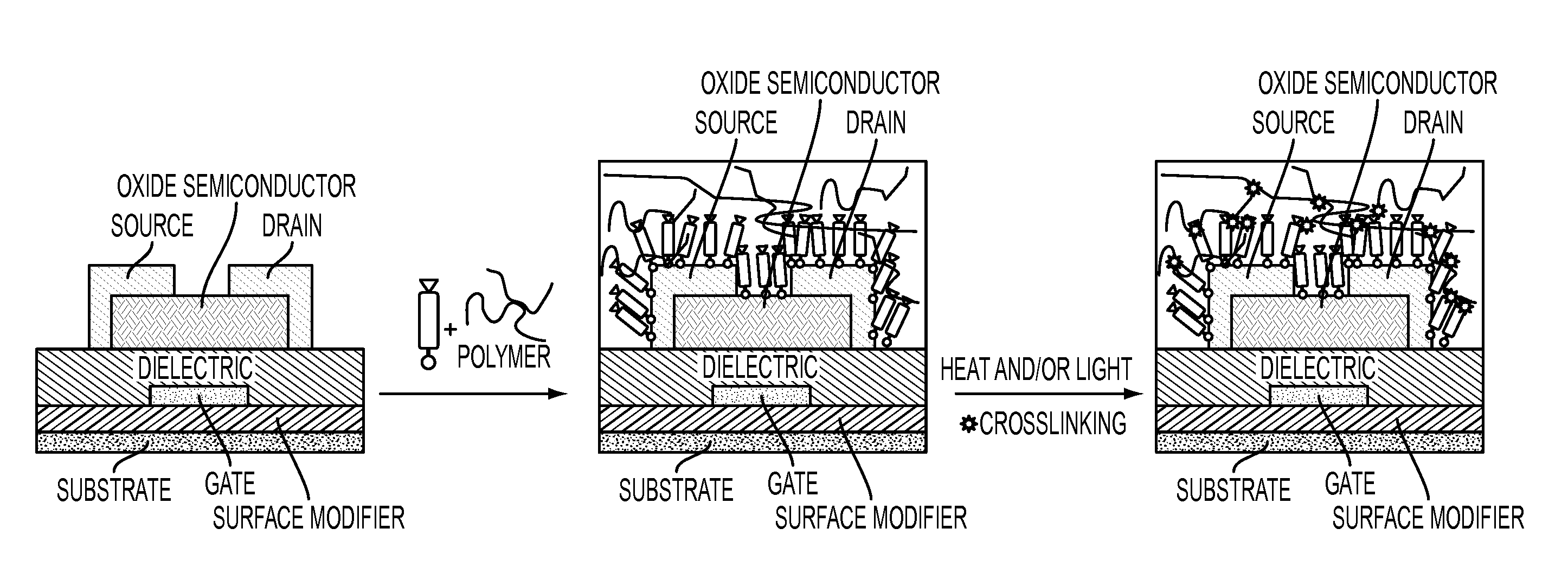
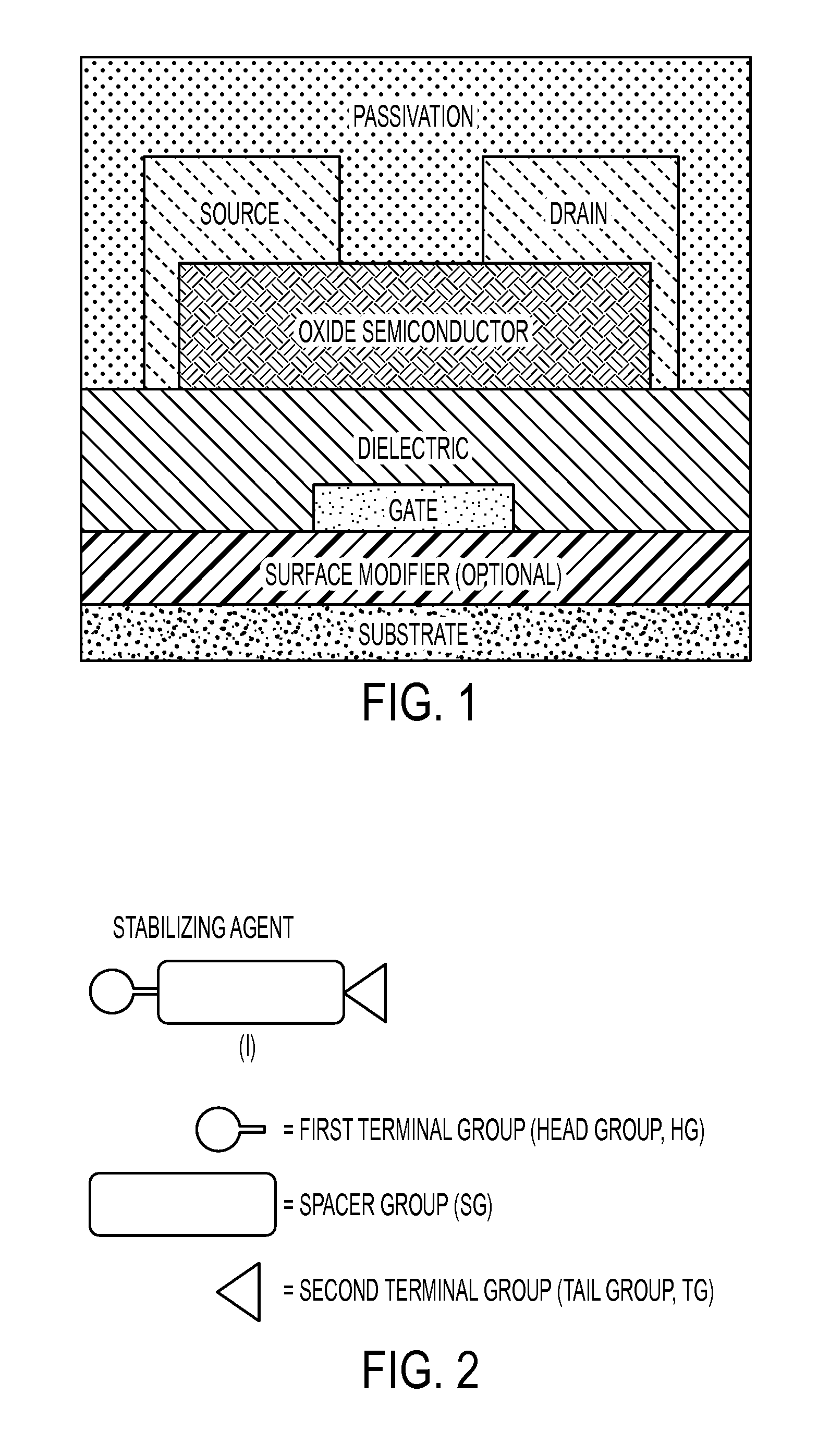
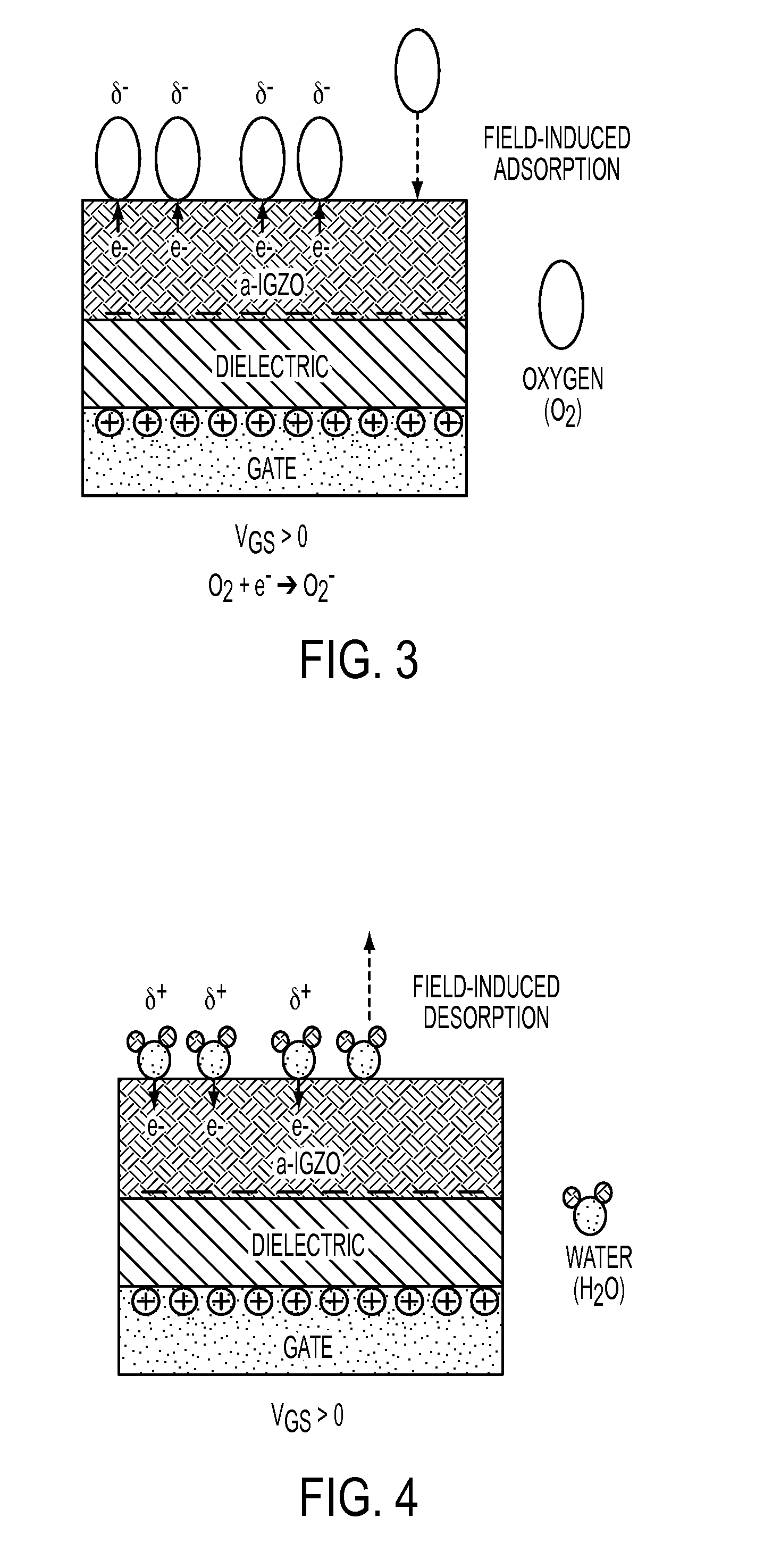
Coating Materials for Oxide Thin Film Transistors
a technology of oxide thin film transistors and coating materials, which is applied in the direction of transistors, electrical devices, semiconductor devices, etc., can solve the problems of unreliable device operation of igzo tfts, degradation of electrical characteristics of igzo tfts, and non-uniformity, so as to improve device stability, improve the adhesion, and improve the effect of surface dehydration
- Summary
- Abstract
- Description
- Claims
- Application Information
AI Technical Summary
Benefits of technology
Problems solved by technology
Method used
Image

Examples
example 1
Bias Temperature Stress Test
[0078]Bottom-gate top-contact IGZO transistor devices were fabricated on a glass substrate with a 250-nm thick Ti / Al / Ti gate metal electrode deposited by sputtering. A 200-nm thick silicon nitride layer (capacitance of about 33 nF / cm2) was then deposited as a gate dielectric by plasma-enhance chemical vapor deposition. The a-IGZO channel was deposited by sputtering using a polycrystalline IGZO target, yielding a film thickness of about 50 nm. Finally, source and drain electrodes were deposited via sputtering a 250-nm thick Ti / Al / Ti layer and subsequent patterning via photolithography and wet etching. The channel width (W) and length (L) of the TFTs were 20 μm and 5 μm, respectively.
[0079]A passivation layer according to the present teachings were prepared from a composition including a photocrosslinkable polymer and a photocrosslinkable phosphonic acid amphiphilic agent (either at 6% (device 1) or 10% (device 2) by weight of the photocrosslinkable polymer...
example 2
Adhesion Test
[0083]Coating films (500-nm thick) according to the present teachings was prepared from a solution comprising a photocrosslinkable polymer (100 mg) and a photocrosslinkable phosphonic acid amphiphilic agent (at 6% by weight of the photocrosslinkable polymer) in an organic solvent (1 mL), which was spin-coated on ITO substrates by spinning the prepared solution at 1000 rpm for 90 s. The samples were baked immediately at 100° C. for 60 s, and then cured with a flood UV-A exposure of 3000 mJ / cm2 using a Model 2000 Dymax light curing system. The samples were then baked at 220° C. for 1 h in a tube furnace under atmosphere.
[0084]The samples were placed on a rigid, flat surface and the edges secured using tape. Uniform pressure was applied on the cutting tool to make 6 parallel cuts 1 mm apart that penetrated to the substrate surface. This operation was repeated, making further parallel cuts of equal number, crossing the original cuts at 90° to them so that a lattice pattern ...
PUM
| Property | Measurement | Unit |
|---|---|---|
| electron mobility | aaaaa | aaaaa |
| concentration | aaaaa | aaaaa |
| thickness | aaaaa | aaaaa |
Abstract
Description
Claims
Application Information