Temperature Controlled Structured ASIC Manufactured on a 28 NM CMOS Process Lithographic Node

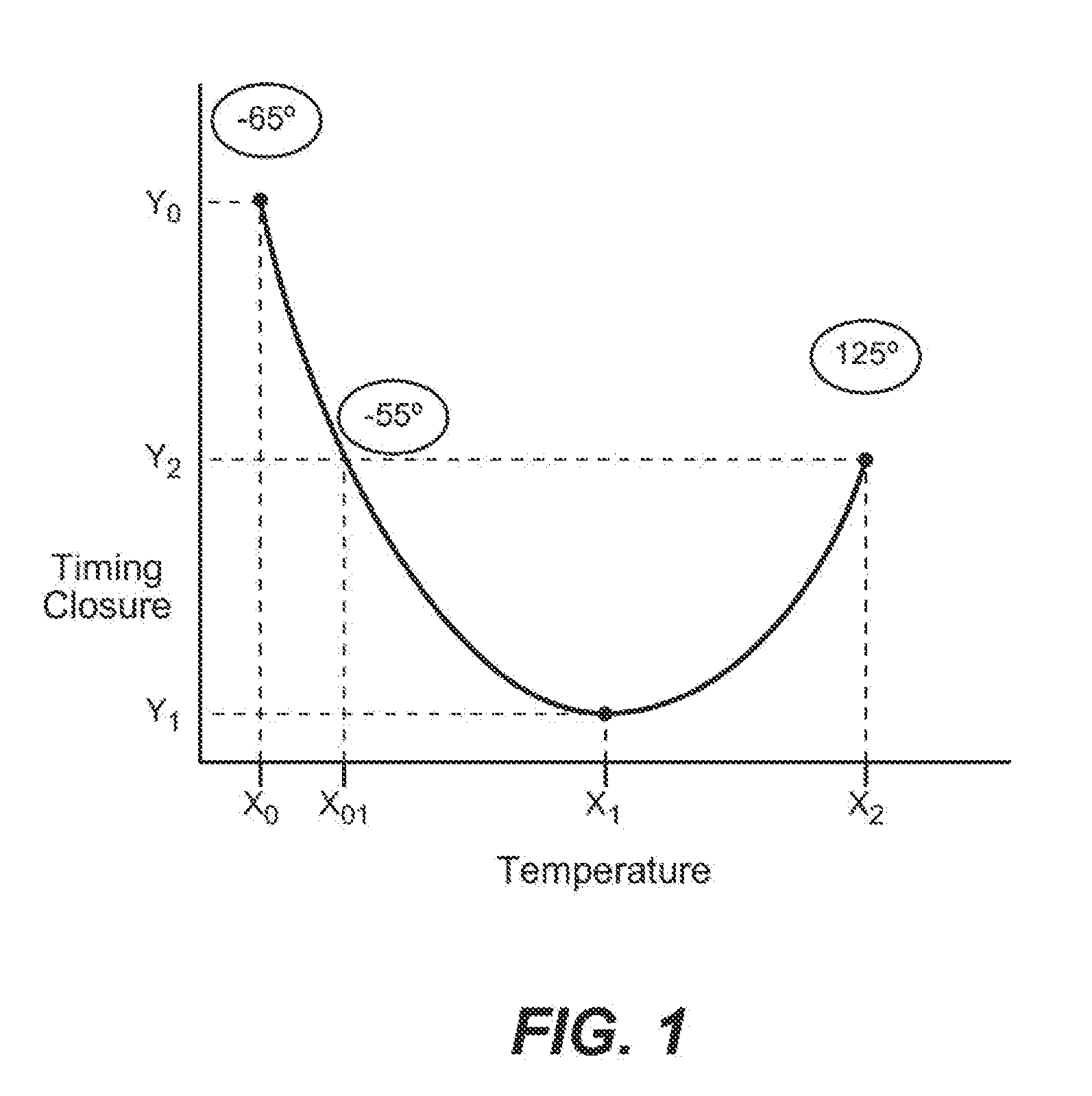
a technology of structured asics and lithographic nodes, which is applied in the direction of process and machine control, instruments, heat measurement, etc., can solve the problems of wasting significant power in transitions within blocks, wasting time and effort, and limiting the maximum performance of the entire system

Inactive Publication Date: 2014-04-17
INTEL CORP
View PDF3 Cites 24 Cited by
  • Summary
  • Abstract
  • Description
  • Claims
  • Application Information

AI Technical Summary

Benefits of technology

[0059]Yet another aspect of the present invention is to provide for a temperature control that will allow a Structured ASIC to achieve timing clos

Problems solved by technology

While the layout of each cell in a standard cell is predetermined, the circuit itself has to be uniquely constructed by connecting all layers to one another and the cells within each layer in a custom manner, which takes time and effort.
The control of any differences and uncertainty in the arrival times of the clock signals can limit the maximum performance of the entire system and create race conditions in which an incorrect data signal may latch within a register.
The clock distribution network often takes a significant portion of the power consumed by a chip; furthermore, significant power can be wasted in transitions within blocks, when their output is not needed.
A simple PLD, historically called a programmable logic device, is much more limited in application, as they do not have a general interconnect structure.
These components are no longer supported by modern EDA (Electronic Design Automation) software and have very limited functionality.
However, optimizing multilevel synthesis logic is more difficult than optimizing two-level synthesis logic, and often employs heuristic techniques.
Design constraints in floorplanning include minimizing the silicon chip area and minimizing timing delay.
The determination of the MRST is in general an NP-complete problem—which is difficult to solve in a reasonable time.
For small numbers of terminals heuristic algorithms exist, but they are expensive in engineering cost to compute.
If a via is disabled, then it cannot practically conduct a signal, i.e., the via has very high resistance or does not physically exist.
If the clock signal arrives at different components at different times, there is clock skew.
Clock skew can be caused by many different things, such as wire-interconnect length, temperature variations and differences in input capacitance on the clock inputs of devices using the clock.
These are also the disadvantages of standard cell ASICs: they are difficult to design, have long development times, and high NRE costs.
The disadvantages of FPGAs are that design size is limited to relatively small production designs, design complexity i

Method used


Image

  • Temperature Controlled Structured ASIC Manufactured on a 28 NM CMOS Process Lithographic Node
  • Temperature Controlled Structured ASIC Manufactured on a 28 NM CMOS Process Lithographic Node
  • Temperature Controlled Structured ASIC Manufactured on a 28 NM CMOS Process Lithographic Node

Examples


Embodiment Construction

[0066]The method and apparatus of the present invention may be described in software, such as the representation of the invention in an EDA tool, or realized in hardwire, such as the actual physical instantiation.

[0067]Regarding the floorplan of the present invention, the drawings sometimes show elements as blocks that in a physical implementation may differ from this stylized representation, but the essential features of the floorplan should be apparent to one of ordinary skill in the art from the teachings herein.

[0068]The elements in the floor plan of the present invention are operatively connected to one another where necessary, as can be appreciated by one of ordinary skill in the art from the teachings herein.

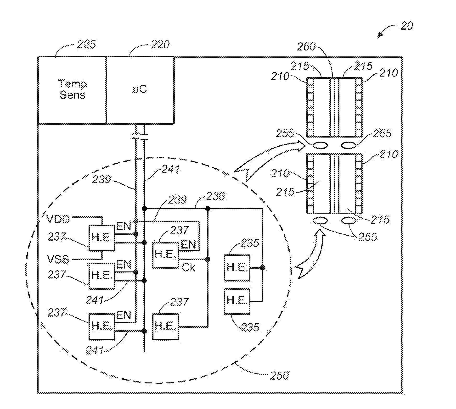
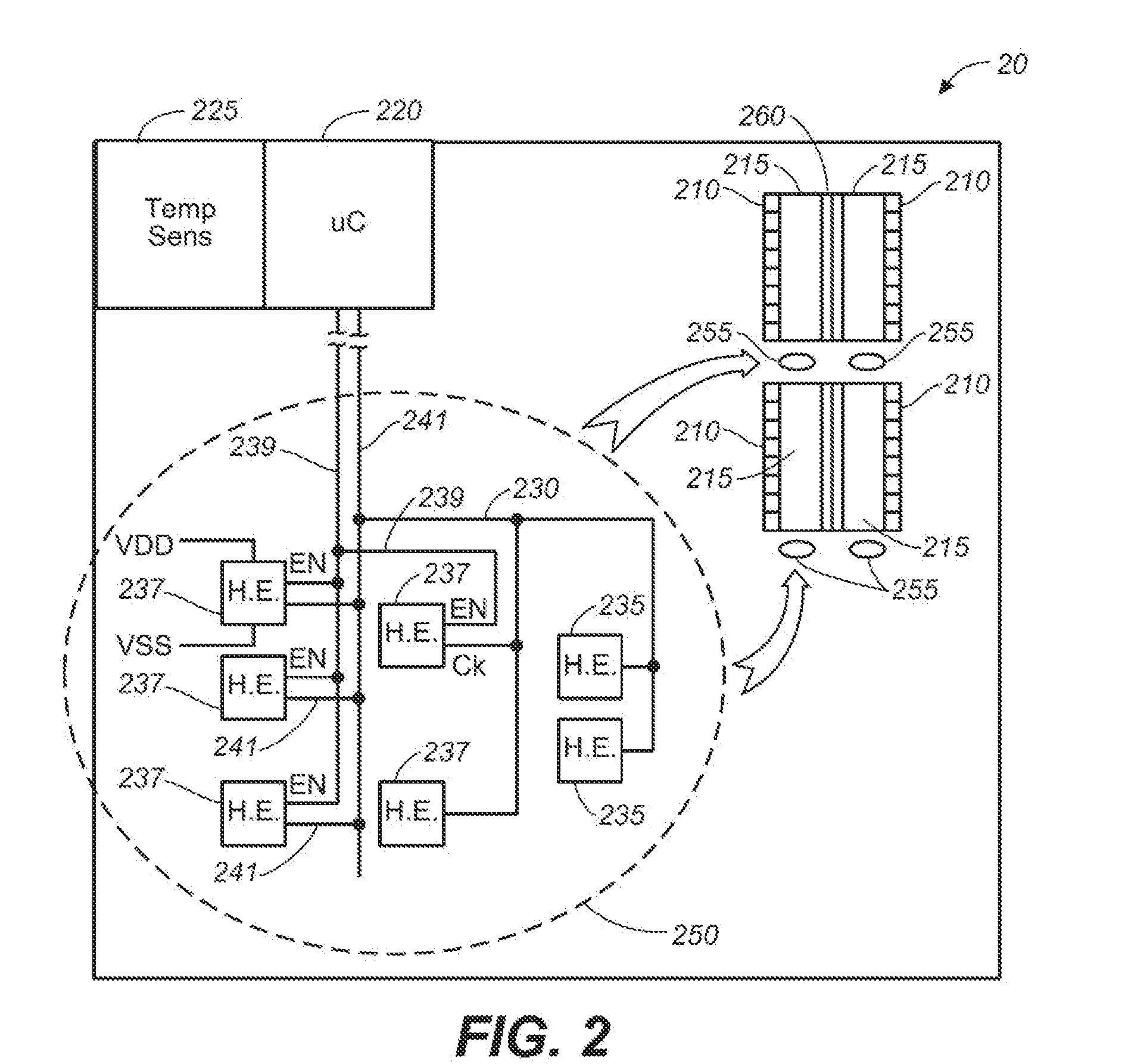
[0069]The temperature control device of the present invention, in particular as shown in the drawings, is for controlling the on-die temperature of a Structured ASIC. Turning attention to FIG. 2 (not to scale), there is shown a Structured ASIC 20 having a substantially re...


PUM


Abstract

A temperature control for a Structured ASIC chip, manufactured using a CMOS process is shown. A circuit employing temperature feedback using a microprocessor and active heating elements, that in a preferred embodiment uses decoupling cell capacitors, is employed to actively heat a die when the temperature of the die drops below a predetermined minimum temperature, in order to achieve timing closure in the chip.

Description

CROSS-REFERENCE TO RELATED APPLICATIONS[0001]The present application is related to: U.S. application Ser. No. ______, Attn. Docket No. EAS 12-1-2 for “VIA-CONFIGURABLE HIGH-PERFORMANCE LOGIC BLOCK INVOLVING TRANSISTOR CHAINS” by Alexander Andreev, Sergey Gribok, Ranko Scepanovic, Phey-Chuin TAN, Chee-Wei KUNG, filed the same day as the present invention, ______ 2012; U.S. application Ser. No. ______, Attn. Docket No. EAS 12-2-2 for “ARCHITECTURAL FLOORPLAN FOR A STRUCTURED ASIC MANUFACTURED ON A 28 NM CMOS PROCESS LITHOGRAPHIC NODE OR SMALLER” by Alexander Andreev, Ranko Scepanovic, Ivan Pavisic, Alexander Yahontov, Mikhail Udovikhin, Igor Vikhliantsev, Chong-Teik LIM, Seow-Sung LEE, Chee-Wei KUNG, filed the same day as the present invention, ______ 2012; US. application Ser. No. ______, Attn. Docket No. EAS 12-3-2 for “CLOCK NETWORK FISHBONE ARCHITECTURE FOR A STRUCTURED ASIC MANUFACTURED ON A 28 NM CMOS PROCESS LITHOGRAPHIC NODE” by Alexander Andreev, Andrey Nikishin, Sergey Gribo...

Claims


Application Information

Patent Timeline
IPC IPC(8): G01K7/01
CPCG01K7/01G01K13/00G05D23/1919G06F1/206
Inventor ANDREEV, ALEXANDERVERITA, MASSIMO
Owner INTEL CORP
Why Eureka
Try Eureka