

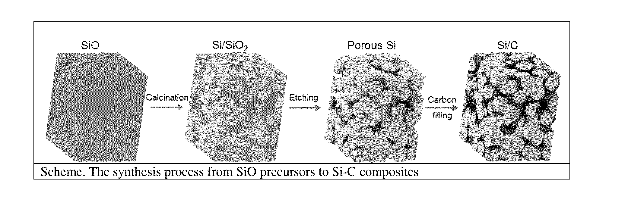
Synthesis of Micro-Sized Interconnected Si-C Composites
a composite material and interconnected technology, applied in the direction of non-aqueous electrolyte accumulator electrodes, cell components, electrochemical treatment, etc., can solve the problems of reducing and affecting the synthesis efficiency of si-c composite materials. , to achieve the effect of good high rate performance, excellent electrochemical performance and high tap density
- Summary
- Abstract
- Description
- Claims
- Application Information
AI Technical Summary
Benefits of technology
Problems solved by technology
Method used
Image

Examples
example 1
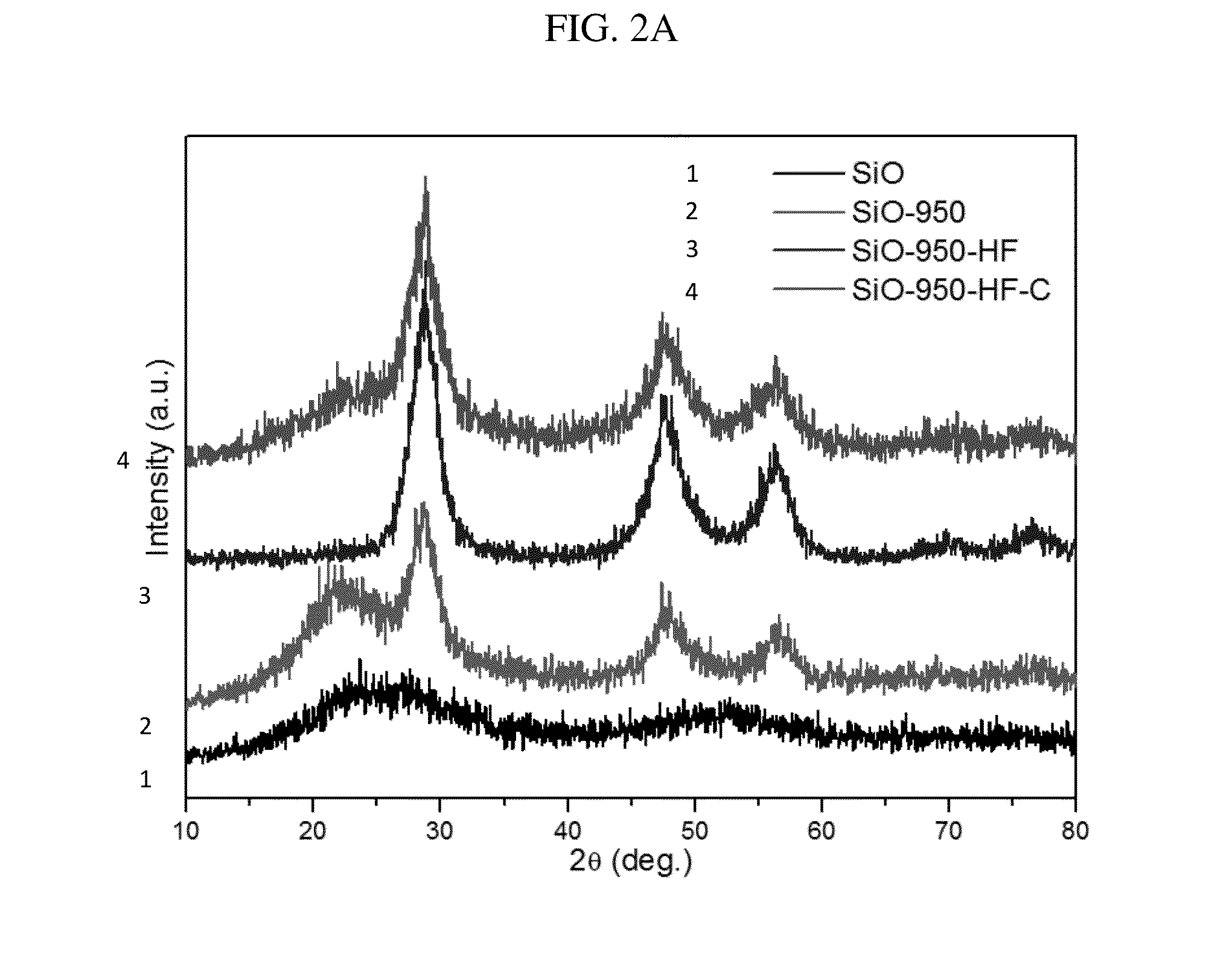
[0065]5 g of commercially available SiO powder (325 mesh) from Aldrich was loaded in an alumina crucible and placed in the center of a horizontal quartz tube followed by Ar purge at a flow rate of 1500 sccm for 20 min. Then the flow rate was reduced to 100 sccm and the tube was heated to 950° C. with a ramping rate of 10° C. / min and kept for 5 h. The samples were taken out of the tube at temperatures below 40° C. Then the samples were immersed in HF at room temperature for 3 h to remove SiO2. The obtained powder was collected by filtration and washed with distilled water and absolute ethanol in sequence several times. The final product was dried in a vacuum box at 60° C. for 4 h, thereby preparing porous silicon.
example 2
[0066]2 g of the porous silicon prepared as in Example 1 was loaded in an alumina crucible and placed in the center of a horizontal quartz tube followed by Ar purge at a flow rate of 1500 sccm for 20 min. Then a mixture of Ar / acetylene flow rate was introduced at a flow rate of 100 sccm and the tube was heated to 620° C. with a ramping rate of 10° C. / min and kept for 20 min. The samples were taken out of the tube at temperatures below 40° C., thereby preparing the Si—C composite.
[0067]Heteroatomic Elemental Doping of the Porous Silicon
[0068]The preparation procedures of heteroatomic doped micro-sized Si—C composite (for example, boron-doped or germanium doped) are the same for Si—C composite, except a mixture of SiO powder and oxide powder (for example, B2O3), with molar ratio of Si:B as 10:1 was used as the starting material. In other embodiments the molar ratio of Si:B may range from 10:1 to 100:1. The products before and after carbon coating are designated B-doped silicon and B-d...
example 3
[0072]The Si—C composite prepared according to Example 2, carbon black (Super P) and poly(acrylic acid) (PAA) were mixed in a weight ratio of 6:2:2 to prepare a slurry. The slurry was coated on a Cu foil current collector using a doctor blade. The resultant Cu foil coated with the slurry was dried in vacuum at 80° C. for 2 h, thereby preparing an anode.
PUM
| Property | Measurement | Unit |
|---|---|---|
| temperature | aaaaa | aaaaa |
| wt % | aaaaa | aaaaa |
| size | aaaaa | aaaaa |
Abstract
Description
Claims
Application Information