Silicon-germanium light-emitting element

a technology of light-emitting elements and silicon-germanium, which is applied in the direction of semiconductor lasers, semiconductor devices, electrical devices, etc., can solve the problems of enormous industrial value, difficult to find out enormous difficulty in the establishment of energy conservation laws, and inability to find enormous difficulties in establishing conservation laws, etc., to achieve easy formation, high luminous efficiency, and low cost of providing light-emitting elements

Inactive Publication Date: 2014-06-26
HITACHI LTD
View PDF3 Cites 11 Cited by
  • Summary
  • Abstract
  • Description
  • Claims
  • Application Information

AI Technical Summary

Benefits of technology

[0066]According to the present invention, it is possible to inexpensively provide the light-emitting element which is higher in the luminous efficiency of the silicon light-emitting element or germanium light-emitting element which can be readily formed on the substrate of silicon or the like. In addition, likewise, it is possible to inexpensively provide the light-emitting element in which the degree of freedom of the design is increased by the stronger light emission source of the silicon laser or the germanium laser which can be readily formed on the substrate of silicon or the like.

Problems solved by technology

Therefore, its industrial value is enormous.
This is because the degree of difficulty in manufacturing the light-emitting element by germanium is higher than that in an on-chip formation of the silicon light-emitting element, but is much lower than that in an on-chip formation of the compound semiconductor light-emitting element.
For the integration of the light-emitting elements, it is desirable to cause either silicon or germanium to efficiently emit light, which is not easy because germanium and silicon have an indirect transition band structure.
It is thus impossible to find out an enormous difficulty in the establishment of the conservation law of energy.
Therefore, it is known that the luminous efficiency is extremely low in silicon or germanium as the indirect transition semiconductor.
However, there is a problem that if, for example, silicon having such a structure as the nanoparticle is formed, then, a surface of the silicon nanoparticle is oxidized to form a silicon dioxide on the surface due to the feature that a silicon surface is extremely easy to oxidize.
Since the silicon dioxide is an insulator which is extremely large in band gap, there is caused a problem that if the silicon dioxide is formed on the surface, then, the electrons or the holes cannot be efficiently implanted.
Therefore, in the conventional light-emitting element, there is a problem that even if a high intensity is obtained in photoluminescence, the efficiency is extremely reduced in electroluminescence.
However, in the nanoparticle formed by a Chemical Vapor Deposition (CVD) or in the structure in which a large number of irregular holes are opened by the anodic oxidation, there is a problem that its crystallinity is lower compared to the single crystal.
However, in the light emission utilizing the defects, there is a problem that with low crystallinity it is impossible to manufacture the element which withstands actual use such as the information communication.
As has been described, although the effort for making silicon emit light has been made by the various techniques such as porous silicon, the nanoparticle, and the Er doping, the luminous efficiency has not so high as to reach the practical level.
The interaction acting between the electrons is called the electron correlation, and becomes a large problem in many transition metallic oxides including the high-temperature super-conduction.
However, when the electrons are confined in such an extremely narrow region that the quantum-mechanical effect becomes important, since the coulomb interaction strongly acts on such a case, it will be impossible to disregard such a coulomb interaction between the electrons.
However, since a necessary amount of implanted electrons is not small, this is not simple.

Method used


Image

  • Silicon-germanium light-emitting element
  • Silicon-germanium light-emitting element
  • Silicon-germanium light-emitting element

Examples


example 1

[0097]There will be shown a method in which holes are bored on the both ends of the light-emitting region of the silicon thin film light-emitting element of PTL 1 to form the barrier region for the carriers, thereby obtaining the same effects as those in the double hetero-structure.

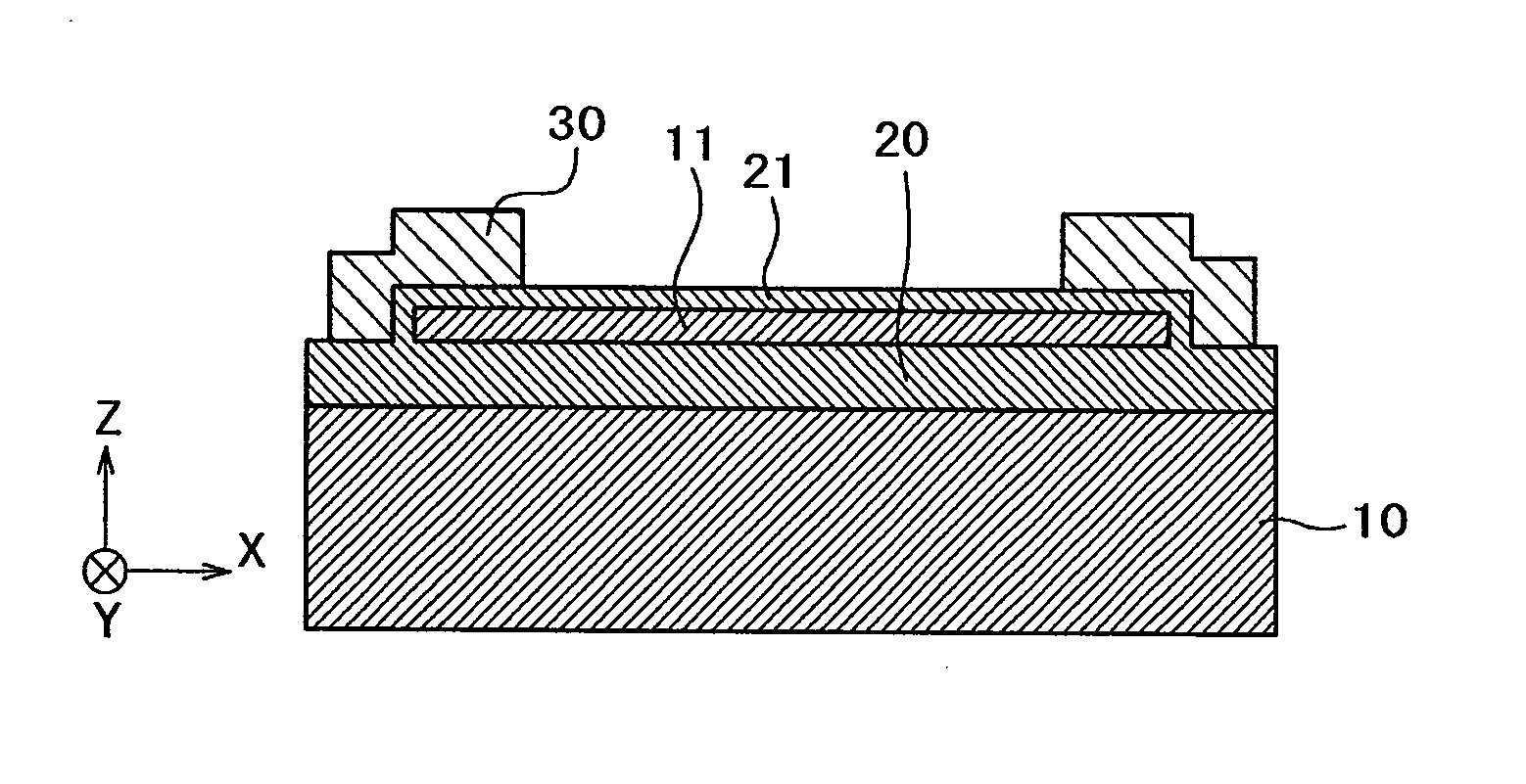
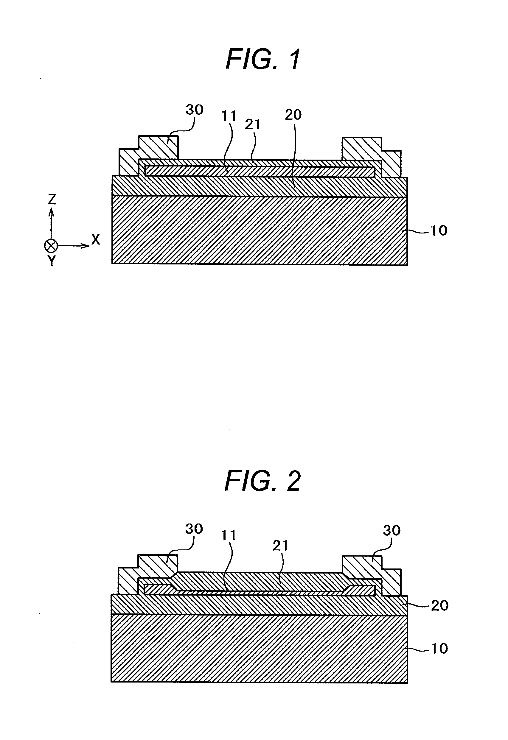
[0098]FIG. 1 is a schematic cross-sectional view in an xy plane of the structure in the middle of manufacture of the silicon thin film light-emitting element. Suppose that a direction vertical to a surface of a silicon supporting substrate 10 and a silicon thin film 11 is set as a z direction, and a direction (a horizontal direction in the figure) in which a current flows through the silicon thin film after completion is set as an x direction. Also, suppose that a depth direction vertical to the paper is set as a y direction. All of figures including this figure are schematic views and ratios in size, and horizontal to vertical ratios in respective regions are different from those in an actual case.

[0099]...

example 2

[0112]There will now be shown a method in which in the fin silicon light-emitting element shown in PTL 2, constriction structures are formed in both ends of the individual silicon thin films composing the fins, and are made the one-dimensional quantum confinement regions to form the barrier regions, thereby obtaining the same effects as those in the double hetero-structure.

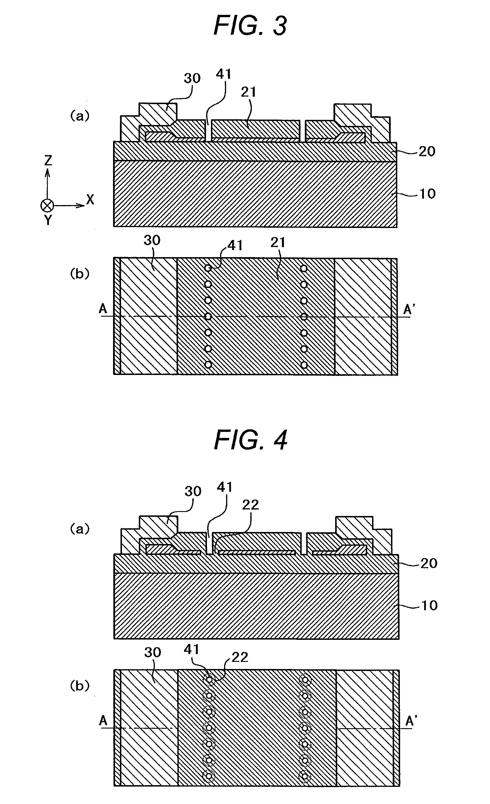
[0113]FIG. 11 shows a finally completed structure of a fin silicon light-emitting element having the constriction structure. A lower figure is a view when viewed from the above of the element, and an upper figure is a cross-sectional view on line A-A′ of the lower figure. However, in the top plan view of the lower figure, for simplicity of the structure, the drawing is made with the silicon oxide film 21 as the protective film being omitted. The silicon oxide film 20 is stacked on the silicon supporting substrate 10, and the silicon thin films 11 are arranged in fins on the silicon supporting substrate 10. The p-t...

example 3

[0127]Although germanium is the indirect transition semiconductor, unlike silicon, the energy level at the point L as the conduction band lowest point, and the energy level at the minimum point which is present at the point T are close to each other. Therefore, if a large amount of electrons are implanted, then, the electrons can be implanted into the point Γ as well. Since the light emission from the point Γ in such a form is obtained in the bulk as well independently of the shape of the element, the germanium light-emitting element may use a thick film. A method is shown in which for this reason the central portions (light-emitting regions) of the individual fins of the fin germanium light-emitting element are thickened, and the end portions to which the electrode are connected are thinned, whereby the barrier regions for the carriers are formed by the quantum confinement effect in the thin portions, thereby obtaining the same effects as those in the double hetero-structure.

[0128]...


PUM

PropertyMeasurementUnit
wavelengthaaaaaaaaaa
thicknessaaaaaaaaaa
band gapaaaaaaaaaa

Abstract

Provided is an element structure whereby it is possible to produce a silicon-germanium light-emitting element enclosing an injected carrier within a light-emitting region. Also provided is a method of manufacturing the structure. Between the light-emitting region and an electrode there is produced a narrow passage for the carrier, specifically, a one-dimensional or two-dimensional quantum confinement region. A band gap opens up in this section due to the quantum confinement, thereby forming an energy barrier for both electrons and positive holes, and affording an effect analogous to a double hetero structure in an ordinary Group III-V semiconductor laser. Because no chemical elements other than those used in ordinary silicon processes are employed, the element can be manufactured inexpensively, simply by controlling the shape of the element.

Description

TECHNICAL FIELD[0001]The present invention relates to a light-emitting element using silicon or germanium, and more particularly to an element structure which is suitable for a high luminosity light-emitting diode or a laser.BACKGROUND ART[0002]In the broad band network bolstering the internet industry, an optical communication is adopted. In transmission and reception of light in this optical communication, a laser using a compound semiconductor of a Group III-V, a Group II-VI or the like is used.[0003]Among various structures proposed in the compound-semiconductor laser, a double hetero-structure is general. The double hetero-structure has a structure where two different kinds of compound semiconductors are used; a compound semiconductor having a smaller band gap is sandwiched by compound semiconductors each having a larger band gap. For the purpose of manufacturing the double hetero-structure, a compound semiconductor of conductivity which is an n-type, a compound semiconductor o...

Claims


Application Information

Patent Timeline
Patent Type & Authority Applications(United States)
IPC IPC(8): H01L33/36
CPCH01L33/0054H01L33/06H01L33/20H01L33/34H01S5/0424H01S5/1032H01S5/3224H01L33/36
Inventor SUWA, YUJISAITO, SHINICHINOMOTO, ETSUKOTAKAHASHI, MAKOTO
Owner HITACHI LTD
Why Eureka
Try Eureka