
Temporary adhesive material for wafer, film for temporary adhesion using same, wafer processing laminate, and method for producing thin wafer using same

Active Publication Date: 2014-11-20
SHIN ETSU CHEM IND CO LTD
View PDF3 Cites 15 Cited by
  • Summary
  • Abstract
  • Description
  • Claims
  • Application Information

AI Technical Summary

Benefits of technology

The invention provides a temporary adhesive material and film that can form a uniform layer on wafers with steps. This leads to easier handling and production of thin wafers without damage. The temporary adhesive layer is removable with low exposure dose without stress, making it suitable for delamination from a support. Overall, this invention allows for improved efficiency and accuracy in the semiconductor industry.

Problems solved by technology

Therefore, the tape has flexibility, but inadequate strength and heat resistance.
The tape is not suited to a step of forming a TSV and a step of forming a wiring layer on a back surface.
This technique requires a very long time for delaminating, so that application of this technique to an actual production process is difficult.
The latter technique is simple because of control only by heating, but does not have sufficient heat stability at a high temperature higher than 200° C. Therefore, the applicable range is narrow.
This technique requires an expensive apparatus such as a laser, and also suffers from a problem in which a processing time per substrate is extended.

Method used


Image

  • Temporary adhesive material for wafer, film for temporary adhesion using same, wafer processing laminate, and method for producing thin wafer using same
  • Temporary adhesive material for wafer, film for temporary adhesion using same, wafer processing laminate, and method for producing thin wafer using same
  • Temporary adhesive material for wafer, film for temporary adhesion using same, wafer processing laminate, and method for producing thin wafer using same

Examples


synthesis example 1

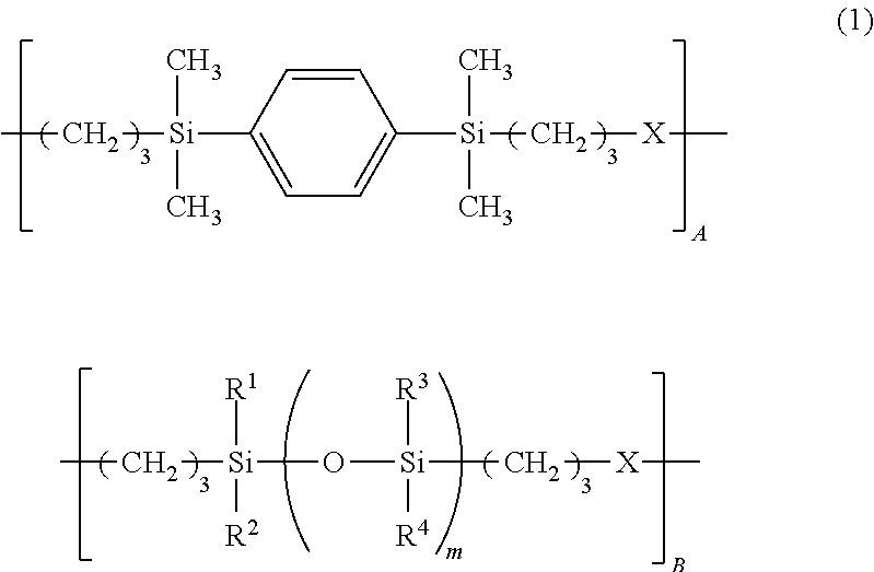
[0148]In a flask equipped with a stirrer, a thermometer, a nitrogen purge system, and a reflux condenser, 43.1 g of 9,9′-bis(3-allyl-4-hydroxyphenyl)fluorene (M-1), 29.5 g of organohydrogenpolysiloxane having an average structural formula (M-3), 135 g of toluene, and 0.04 g of chloroplatinic acid were placed, and heated at 80° C. 17.5 g of 1,4-bis(dimethylsilyl)benzene (M-5) was then added dropwise to the flask over 1 hour. At this time, the temperature in the flask was increased to 85° C. After the completion of dropwise addition, the mixture was aged at 80° C. for 2 hours, toluene was distilled off, and 80 g of cyclohexanone was added, to obtain a resin solution (A-1) containing cyclohexanone as a solvent, and having a resin solid concentration of 50% by mass. The molecular weight of the resin in the solution was determined by GPC, and the weight average molecular weight was 45,000 in terms of polystyrene.

synthesis example 2

[0149]In a 5-L flask equipped with a stirrer, a thermometer, a nitrogen purge system, and a reflux condenser, 396.9 g of compound (M-1) and 45.0 g of compound (M-2) were dissolved in 1,875 g of toluene. 949.6 g of compound (M-3) and 6.1 g of compound (M-4) were then added to the flask, and heated at 60° C. After then, 2.2 g of carbon-supported platinum catalyst (5% by mass) was added. It was confirmed that the internal reaction temperature was increased to 65 to 67° C. The temperature was then increased to 90° C. for 3 hours, and decreased to 60° C. 2.2 g of carbon-supported platinum catalyst (5% by mass) was added, and 107.3 g of compound (M-5) was added dropwise to the flask over 1 hour. The temperature in the flask was increased to 78° C. After the completion of dropwise addition, the mixture was aged at 90° C. for 3 hours, and cooled to room temperature. 1,700 g of methyl isobutyl ketone (MIBK) was added. The reaction solution was filtered under pressure through a filter to remo...

synthesis example 3

[0150]In a 5-L flask equipped with a stirrer, a thermometer, a nitrogen purge system, and a reflux condenser, 84.1 g of epoxy compound (M-2) was dissolved in 600 g of toluene. 294.6 g of compound (M-3) and 25.5 g of compound (M-4) were then added to the flask, and heated at 60° C. After then, 1 g of carbon-supported platinum catalyst (5% by mass) was added. It was confirmed that the internal reaction temperature was increased to 65 to 67° C. The temperature was then increased to 90° C., and the mixture was aged for 3 hours and cooled to room temperature. 600 g of methyl isobutyl ketone (MIBK) was added. The reaction solution was filtered under pressure through a filter to remove the platinum catalyst. The solvent in the resin solution was distilled under reduced pressure and 270 g of cyclopentanone was added to obtain a resin solution (A-3) containing cyclopentanone as a solvent, and having a solid content concentration of 60% by mass. The molecular weight of the resin in the resin ...


PUM

PropertyMeasurementUnit
Thicknessaaaaaaaaaa
Thicknessaaaaaaaaaa
Adhesion strengthaaaaaaaaaa

Abstract

A temporary adhesive material for a wafer includes a first temporary adhesive layer of a silicone-containing polymer layer containing a photo base generator and a second temporary adhesive layer of a silicone-containing polymer layer which is laminated on the first temporary adhesive layer, does not contain the photo base generator, and is different from the polymer layer. Thereby, there can be formed a temporary adhesive layer having high thickness uniformity, even on a wafer having a step. Because of the thickness uniformity, a thin wafer having a uniform thickness of 50 μm or less can be easily obtained. When a thin wafer is produced and then delaminated from a support, the wafer can be delaminated from the support by exposure at a low exposure dose without stress. Therefore, a brittle thin wafer can be easily handled without causing damage, and a thin wafer can be easily produced.

Description

TECHNICAL FIELD[0001]The present invention relates to a temporary adhesive material for a wafer capable of effectively obtaining a thin wafer, a film for temporary adhesion using the same, a wafer processing laminate, and a method for producing a thin wafer.BACKGROUND ART[0002]Three-dimensional semiconductor mounting has become essential for further higher density, higher capacity, higher speed, and low power consumption. A three-dimensional semiconductor mounting technique is a semiconductor production technique by thinning a semiconductor chip, and connecting the chip to another chip using a through silicon via (TSV) to form a multilayer. In order to realize this technique, a step of grinding a surface without a circuit (also referred to as “back surface”) of a substrate on which a semiconductor circuit is formed to thin the substrate, and forming an electrode including a TSV on the back surface is required.[0003]Conventionally, in a step of grinding the back surface of a silicon ...

Claims


Application Information

Patent Timeline
IPC IPC(8): H01L21/683C09J183/14H01L21/304
CPCH01L21/6836H01L21/304C09J2203/326C09J2201/36C09J183/14C08G77/14C08G77/52C08K5/0025C08K5/205C09J2301/1242C09J2301/208C09J2301/408C09J2301/416C09J2483/00H01L21/6835H01L2221/68327H01L2221/6834H01L2221/68381Y10T428/2852Y10T428/287C09J7/203C09J7/22C09J183/04H01L21/683
Inventor YASUDA, HIROYUKISUGO, MICHIHIRO
Owner SHIN ETSU CHEM IND CO LTD
Learn More