
Highly Selective Nanostructure Sensors and Methods of Detecting Target Analytes

a nanostructure sensor and target analyte technology, applied in the field of sensing devices, can solve the problems of fundamental challenges and deficiencies in such prior attempts, severely limit the usability of such conventional sensors, and pose long-term reliability problems, and achieve the effect of increasing conductivity

Active Publication Date: 2015-09-24
GEORGE MASON UNIVERSITY +3
View PDF0 Cites 16 Cited by
  • Summary
  • Abstract
  • Description
  • Claims
  • Application Information

AI Technical Summary

Benefits of technology

The present invention describes highly selective and sensitive sensors that use semiconductor nanostructures decorated with metal and / or metal-oxide nanoclusters or particles. These sensors have several advantages over conventional sensors including low-power operation, longer lifetime, fast on / off capability, wide sensing range, fast response and recovery, and reliable and repeatable operation. The invention also provides hybrid chemiresistive architectures utilizing nanoengineered wide-bandgap semiconductor backbone functionalized with multicomponent photocatalytic nanoclusters of metal-oxides and / or metals. These sensors can detect selected compounds and provide a reliable and repeatable operation for economical, multianalyte single-chip sensors. The nanoparticle clusters are multicomponent clusters comprising first metal-oxide nanoparticles and second metal nanoparticles. The nanostructure has a first bandgap, and the nanoparticle clusters have a second bandgap equal to or less than the first bandgap. The devices exhibit increased conductivity upon exposure to the target analyte in the presence of radiation, including light and / or visible light.

Problems solved by technology

As such, the usability of such conventional sensors is severely limited and poses long-term reliability problems.
Although such results demonstrate the potentials of the nanowire-nanocluster based hybrid sensors, fundamental challenges and deficiencies in such prior attempts remain.
Although such mats may increase sensitivity, the complex nature of inter-wire conduction makes interpreting the results difficult.
Also, room-temperature operation of such previous sensors has not been demonstrated, and the selectivity is shown for only a very limited number of chemicals.
Further, the reported sensitivities of such conventional devices were quite low even with long response times. Further, such conventional devices typically do not provide for air as the carrier gas.
Thus, such demonstrations have resulted in poor selectivity of known chemical sensors, and therefore have not resulted in commercially viable gas sensors.
Detecting traces of explosives is challenging, however, because of the low vapor pressures of most explosives (Moore, D S (2004) “Instrumentation for trace detection of high explosives,” Review of Scientific Instruments 75(8):2499-2512; Yinon J (2002) “Field detection and monitoring of explosives,” TrAC Trends in Analytical Chemistry 21(4):292-301; Senesac L. and Thundat T G (2008) “Nanosensors for trace explosive detection,” Materials Today 11(3):28-36.
Moreover, the difficulty of explosive detection is aggravated by the noisy environment which masks the signal from the explosive, the potential for high false alarms, and the need to determine a threat quickly.
As such, trained canine teams remain the most reliable means of detecting explosive vapors to date; however, dogs are expensive to train and tire easily.
This is extremely challenging as most semiconductor-based sensors use metal-oxides (such as SnO2, In2O3, ZnO) as the active elements, which are limited due to the non-selective nature of the surface adsorption sites.
The surface / adsorbate interactions of conventional sensor structures are limited and non-specific.
Thus, conventional sensor devices lack the same selectivity as their bulk-counterpart devices.

Method used


Image

  • Highly Selective Nanostructure Sensors and Methods of Detecting Target Analytes
  • Highly Selective Nanostructure Sensors and Methods of Detecting Target Analytes
  • Highly Selective Nanostructure Sensors and Methods of Detecting Target Analytes

Examples


example 1

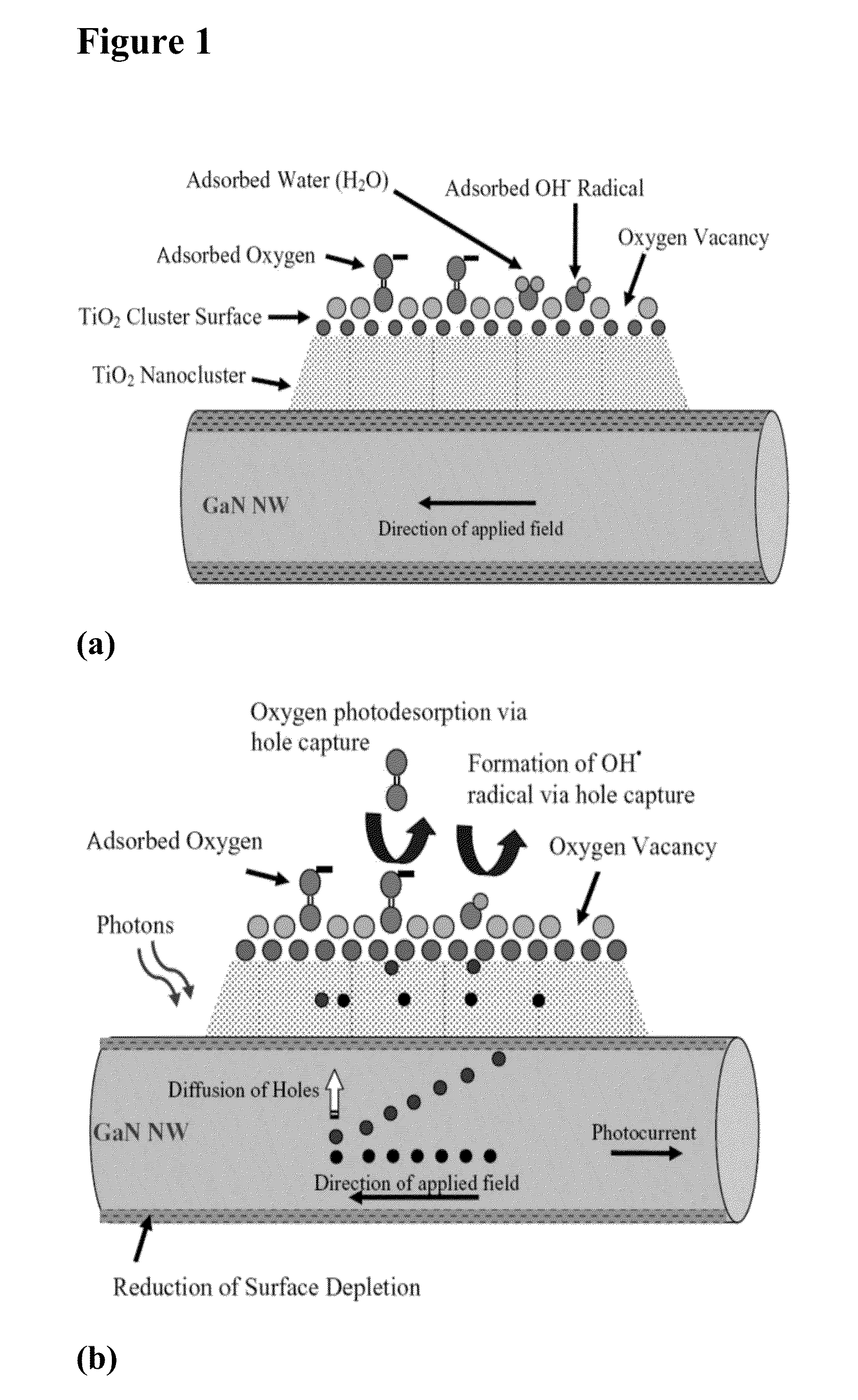
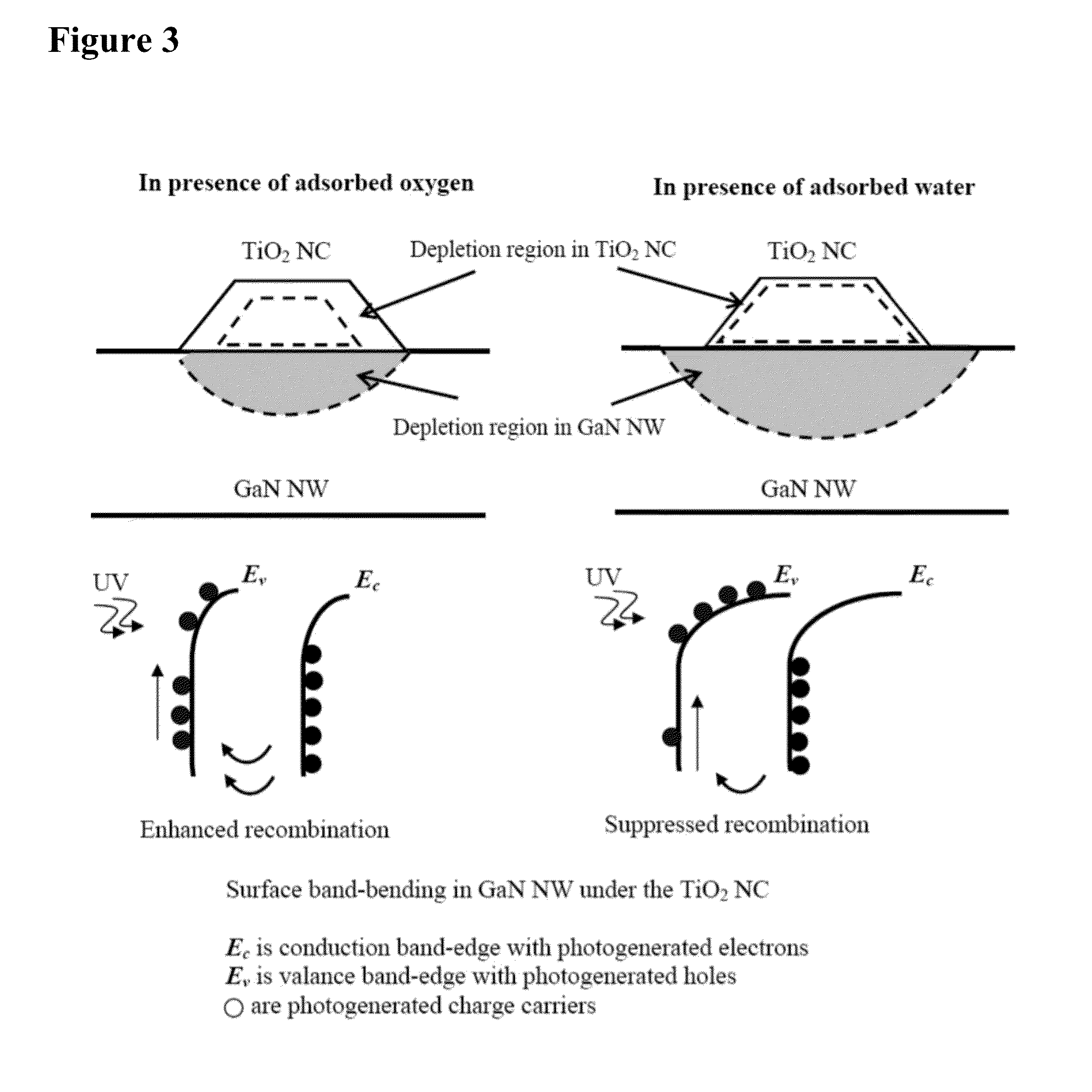
[0153]Nanowire-nanocluster hybrid chemical sensors were realized by functionalizing gallium nitride (GaN) nanowires (NWs) with titanium dioxide (TiO2) nanoclusters for selectively sensing benzene and other related aromatic compounds.

[0154]Materials and Methods

[0155]C-axis, n-type, Si-doped GaN grown by catalyst-free molecular beam epitaxy on Si (111) substrates were utilized. For details of NW growth, see Bertness K A et al. (2008) “Mechanism for spontaneous growth of GaN nanowires with molecular beam epitaxy” J. Crystal Growth 310(13):3154-3158). The process of sensor fabrication is shown in FIG. 19. Post-growth device fabrication was done by dielectrophoretically aligning the nanowires on 9 mm×9 mm sapphire substrates (see Motayed A et al. (2006) “Realization of reliable GaN nanowire transistors utilizing dielectrophoretic alignment technique,” J. Appl. Phy. 100:114310). The device substrates had 12 nm thick Ti alignment electrodes of semi-circular geometry with gaps between them ...

example 2

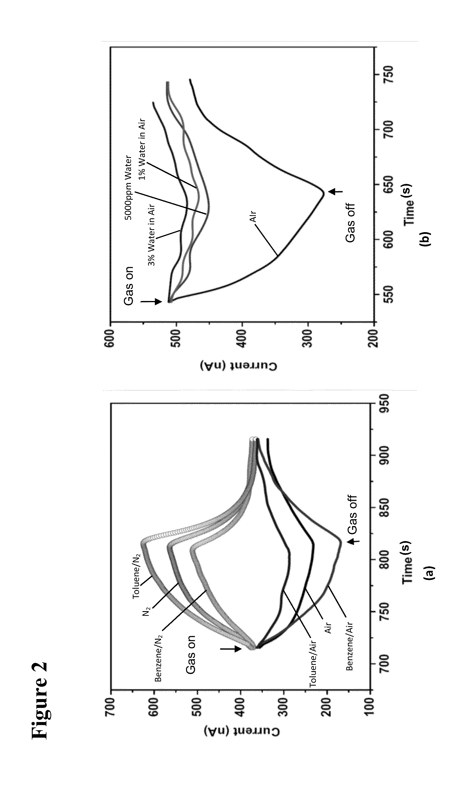
[0172]The sensing behavior of three NWNC based hybrid sensors is compared: 1) GaN NW coated with TiO2 NCs (hereafter referred to as GaN / TiO2 NWNC hybrids); 2) GaN NW coated with TiO2 and Pt multicomponent NCs (i.e., GaN / (TiO2—Pt) NWNC hybrids); and 3) GaN NW coated with Pt NCs (i.e., GaN / Pt NWNC hybrids). It was found that sensors with TiO2—Pt multicomponent NCs on GaN NW were only sensitive to methanol, ethanol, and hydrogen. Higher carbon-containing alcohols (such as n-propanol, iso-propanol, n-butanol) did not produce any sensor response. These sensors had the highest sensitivity towards hydrogen. Prior to the Pt deposition, the GaN / TiO2 NWNC hybrids did not exhibit any response to alcohols, however they detected benzene and related aromatic compounds such as toluene, ethylbenzene, xylene, and chlorobenzene mixed with air. The GaN / Pt hybrids only showed sensitivity to hydrogen and not to methanol or ethanol. The sensitivity of GaN / Pt hybrids towards hydrogen was lower compared to...

example 3

[0195]Alcohol sensors using gallium nitride (GaN) nano-wires (NWs) functionalized with zinc oxide (ZnO) nanoparticles are demonstrated. These sensors operate at room temperature, are fully recoverable, and demonstrate a response and recovery time on the order of 100 seconds. The sensing is assisted by UV light within the 215-400-nm band and with the intensity of 375 nW / cm2 measured at 365 nm. The ability to functionalize an inactive NW surface, with analyte-specific active metal-oxide nanoparticles, makes this sensor suitable for fabricating multianalyte sensor arrays.

[0196]Methods and Materials

[0197]Si-doped c-axis n-type GaN NWs were grown using catalyst-free molecular beam epitaxy on Si (111) substrate as described in Bertness K A et al. (2008), supra, J. Cryst. Growth 310(13):3154-3158. The NW diameter and length are in the ranges of 250-350 nm and 21-23 μm, respectively. The GaN NWs were detached from the substrate by sonication in isopropanol and dielectrophoretically aligned ...


PUM


Abstract

A nanostructure sensing device comprises a semiconductor nanostructure having an outer surface, and at least one of metal or metal-oxide nanoparticle clusters functionalizing the outer surface of the nanostructure and forming a photoconductive nanostructure / nanocluster hybrid sensor enabling light-assisted sensing of a target analyte.

Description

CROSS-REFERENCE TO RELATED APPLICATIONS[0001]This application is based on U.S. Provisional Patent Application Ser. No. 61 / 623,957, filed Apr. 13, 2012, Application Ser. No. 61 / 625,511, filed Apr. 17, 2012, Application Ser. No. 61 / 730,865, filed Nov. 28, 2012, and Application Ser. No. 61 / 775,305, filed Mar. 8, 2013, which applications are all incorporated herein by reference in their entireties and to which priority is claimed.STATEMENT REGARDING FEDERALLY SPONSORED RESEARCH OR DEVELOPMENT[0002]This work was supported by the National Science Foundation (NSF) under ECCS-0901712 grant, by the Defense Threat Reduction Agency (DTRA) under HDTRA11010107, and by the National Institute of Standards and Technology (NIST) under SB134110SE0579 and SB134111SE0814. The US government has certain rights in this invention.FIELD OF THE INVENTION[0003]The present invention relates to a sensing device including a semiconductor nanostructure and at least one of metal or metal-oxide nanoparticles functi...

Claims


Application Information

Patent Timeline
IPC IPC(8): G01N33/00
CPCG01N33/0031G01N27/3278G01N27/4146
Inventor MOTAYED, ABHISHEKALURI, GEETHADAVYDOV, ALBERT V.RAO, MULPURI V.OLESHKO, VLADIMIR P.BAJPAI, RITUZAGHLOUL, MONA E.
Owner GEORGE MASON UNIVERSITY
Learn More