

Layer structure for a group-iii-nitride normally-off transistor
a group-iii-nitride, normally-off technology, applied in the direction of transistors, electrical devices, semiconductor devices, etc., can solve the problems of limited reduction of on-state resistance, low drain current, and ineffective use of normally-on hfets for actual power switching applications, so as to reduce tensile strain, improve tensile quality, and improve tensile quality
- Summary
- Abstract
- Description
- Claims
- Application Information
AI Technical Summary
Benefits of technology
Problems solved by technology
Method used
Image

Examples
second embodiment
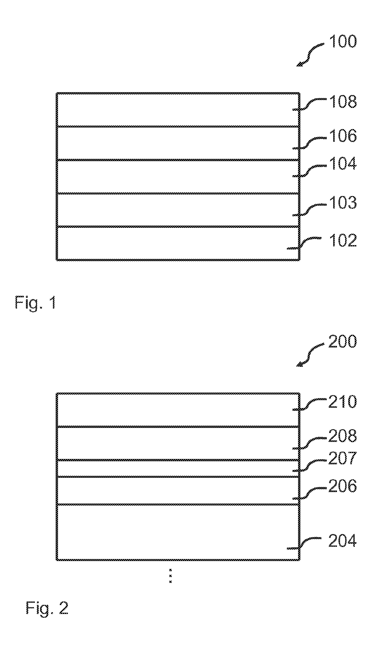
[0084]FIG. 2 shows a schematic illustration of a layer structure 200 according to a The buffer-layer structure is omitted from the figure. The structure is similar to that of FIG. 1 in that it has a back-barrier layer 204, a channel layer 206, and an electron-supply layer 208. The present embodiment differs from that of FIG. 1 in the addition of a spacer layer 207 between the channel layer 206 and the electron-supply layer 208. In the present embodiment, the spacer layer 207 is made of AlN and has a thickness of 3 nm at most, preferably only 1 to 2 nm. In a variant, the spacer layer is made of AlGaN. Any Al mole fraction larger than 35% is suitable. Furthermore, on top of the electron-supply layer, a cap layer 210 is provided. The cap layer 210 is in the present embodiment made of GaN. It may alternatively be made of InGaN. The thickness of the cap layer is between 2 and 10 nm, preferably 4 nm.
[0085]In all embodiments of the present specification, the spacer layer 207 is an optiona...
third embodiment
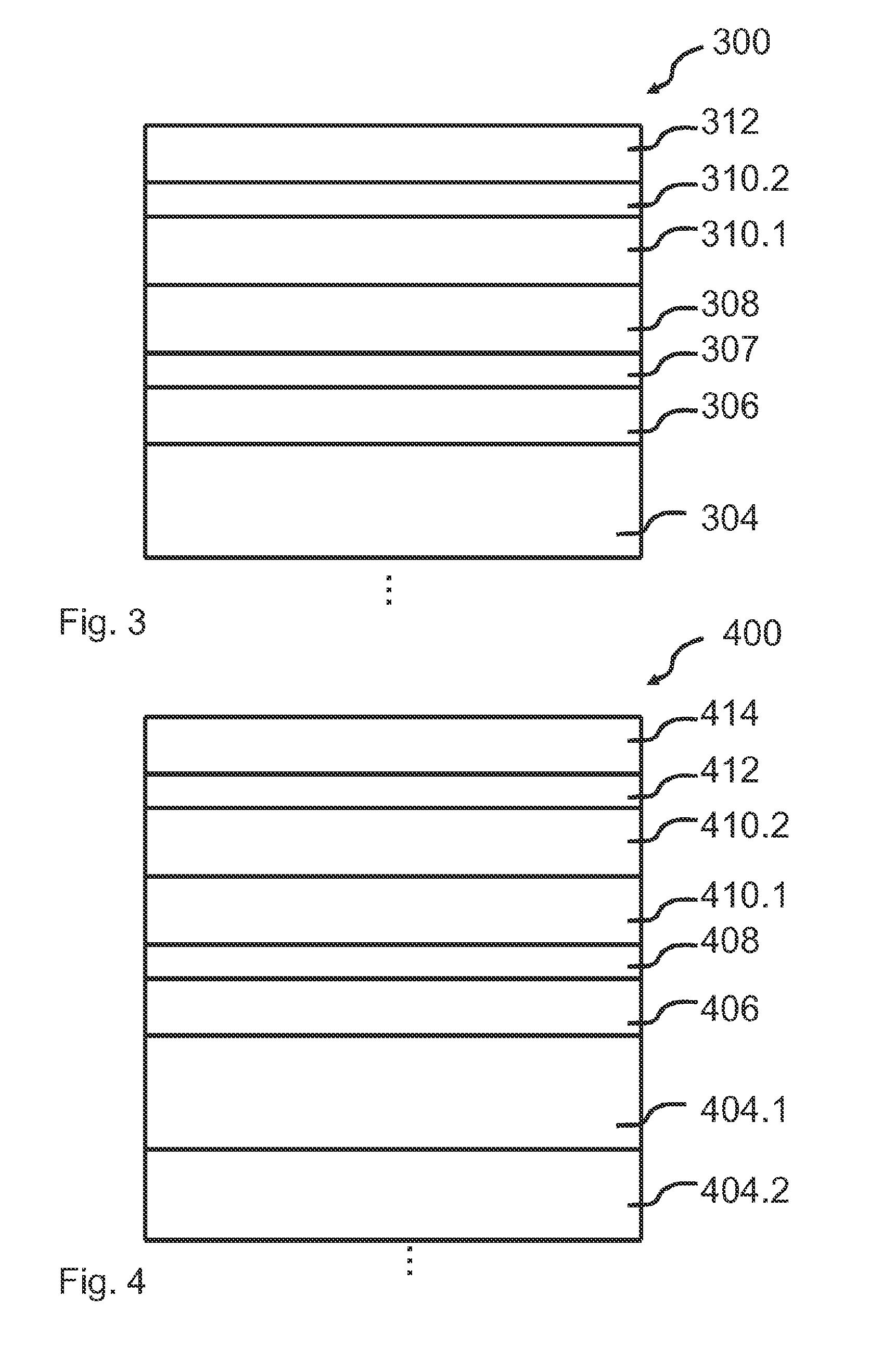
[0087]FIG. 3 shows a schematic illustration of a layer structure 300 according to a The buffer-layer structure is not shown. The structure is similar to that of FIG. 2 in that it has a back-barrier layer 304, a channel layer 306, a spacer layer 308, an electron-supply layer 310 and a cap layer 312. It differs from the embodiment of FIG. 2 in that the electron-supply layer is compositionally graded. In the present embodiment, the electron-supply layer comprises two sublayers 310.1 and 310.2. However, the structure may be varied to comprise a larger number of sublayers. The present embodiment is an example of a layer structure, in which the compositional grading of the electron-supply layer achieves a decrease of the band gap of the electron-supply layer 310 with increasing distance from the channel layer 306. Specifically, in the present embodiment, the first sublayer 310.1 has a larger band gap than the second sublayer 310.2. For in-stance, the first sublayer 310.1 is made of AlGaN...
fourth embodiment
[0090]FIG. 4 shows a schematic illustration of a layer structure 400 according to a Again, the buffer-layer structure is not shown. The layer structure 400 is similar to that of FIG. 3 in that it has a back-barrier layer 404, a channel layer 406, a spacer layer 408, an electron-supply layer 410 made of two sublayers 410.1 and 410.2, and a cap layer 412.
[0091]The layer structure 400 of FIG. 4 differs from the embodiment of FIG. 3 in the addition of a dielectric layer 414 on the cap layer, and in that the back-barrier layer is also compositionally graded.
[0092]The dielectric layer 414 is preferably a high-K material. Suitable dielectric materials are hafnium-based dielectrics such as HfO2 or HfSiON, zirconium-based dielectrics such as ZrO2 or zirconium silicate, Al2O3, SiON, or Si3N4. It has a thickness of between 5 and 25 nm, preferably between 7 and 20 nm.
[0093]In the present embodiment, the back-barrier layer 404 comprises two sublayers 404.1 and 404.2. However, the structure may ...
PUM
 Abstract
Description
Claims
Application Information