Hybrid Perovskite with Adjustable Bandgap

a technology of perovskite and bandgap, which is applied in the field of hybrid perovskite materials, can solve the problems of mixed halogenides, mixed halogenides approach usually does not demonstrate good performance in solar devices, and the cost of increasing complexity and manufacturing pri

Inactive Publication Date: 2016-05-12
SHARP LAB OF AMERICA INC
View PDF1 Cites 28 Cited by
  • Summary
  • Abstract
  • Description
  • Claims
  • Application Information

AI Technical Summary

Benefits of technology

[0018]Disclosed herein is a new perovskite formation pathway to form planar thin films applicable to tandem solar cells with silicon (Si), copper indium gallium selenide (CIGS), or copper zinc tin selenide/sulfide (CZTS) subcells. The bandgap of this perovskite is tunable through A-site cation exchange using formamidinium iodide and ethylammonium iodide to ensure chemical stability. In particular, a thin film lead iodide may be deposited using thermal evaporation

Problems solved by technology

However, this efficiency is gained at the cost of increased complexity and manufacturing price.
However, due to manufacturing costs the primary research interest has been devoted to tandem solar cells that utilized mature technologies such as Si, copper indium gallium selenide (CIGS), or even the more problematic copper zinc tin selenide/sulfide (CZTS) as a bottom subcell.
However, despite the promise of such a simple technique, it has recently been found that there is a fundamental problem with the use of such mixed halogenides.
Therefore, the mixed halogenides approach usually does not demonstrate good performance in solar devices, as both current and voltage are low.
Therefore,

Method used


Image

  • Hybrid Perovskite with Adjustable Bandgap
  • Hybrid Perovskite with Adjustable Bandgap
  • Hybrid Perovskite with Adjustable Bandgap

Examples


Embodiment Construction

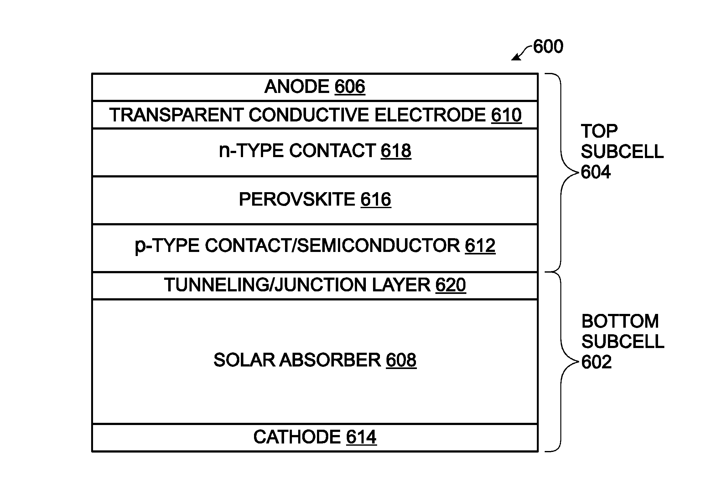
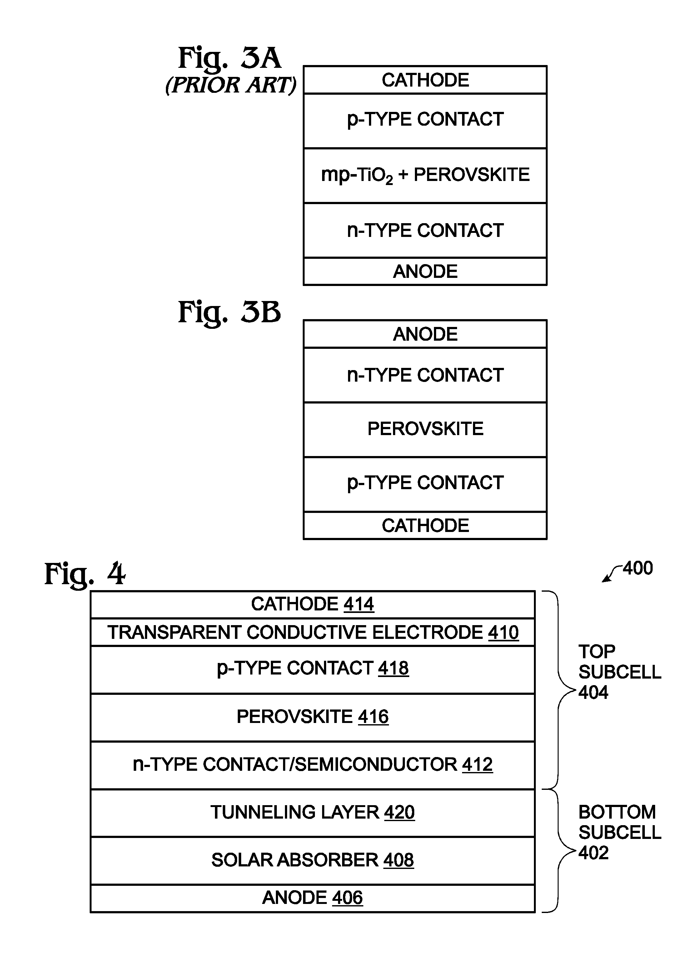
[0033]As used herein, perovskite is a material with the same structure as calcium titanate (CaTiO3), or ABX3. The B cation is in 6-fold coordination forming an octahedron, while A cations occupy interstitial spaces and exhibit 12-fold coordination.

[0034]A semiconductor is a material whose conductivity, due to charges of both signs, is normally in the range between that of metals and insulators and in which the electric charge carrier density can be changed by external means.

[0035]N-type semiconductors have a larger electron concentration than hole concentration. The phrase ‘n-type’ comes from the negative charge of the electron. In n-type semiconductors, electrons are the majority carriers and holes are the minority carriers. N-type semiconductors are created by doping an intrinsic semiconductor with donor impurities. In an n-type semiconductor, the Fermi level is greater than that of the intrinsic semiconductor and lies closer to the conduction band than the valence band.

[0036]As o...


PUM


Abstract

A method is provided for preparing a thin film of perovskite material having an adjustable bandgap. The method forms a thin film of material having the formula BX2, where anionic part X is a halide, and where the cation B is lead (Pb), tin (Sn), or germanium (Ge). A solution is formed of materials with the formulas A1X and A2X, where cation A1 is formamidinium, and where cation A2 is an organic cation having a larger size larger than a methylammonium cation. The method deposits the solution over the BX2 thin film, and forms a perovskite material having the formula A11-YA2yBX3. For example, the A2 cation may be an ammonium cation such as ethylammonium, guanidinium, dimethylammonium, acetamidinium, or substituted derivatives of the above-mentioned ammonium cations. In one aspect, the perovskite material A1BX3 may be formamidinium iodide (FAI), and A2BX3 may be ethylammonium iodide (EtAI). Tandem solar cells are also provided.

Description

RELATED APPLICATIONS[0001]This application is a Continuation-in-part of an application entitled, PLANAR STRUCTURE SOLAR CELL WITH INORGANIC HOLE TRANSPORTING MATERIAL, invented by Alexey Koposov et al, Ser. No. 14 / 320,691, filed on Jul. 1, 2014, Attorney Docket No. untitled SLA3386, which is incorporated herein by reference.BACKGROUND OF THE INVENTION[0002]1. Field of the Invention[0003]This invention generally relates to solar cells and, more particularly, to hybrid perovskite material suitable for use in a tandem solar cell.[0004]2. Description of the Related Art[0005]FIG. 1 is a partial cross-sectional view of an exemplary silicon (Si) solar cell (prior art). Conventional photovoltaic cells are commonly composed of doped silicon with metallic contacts deposited on the top and bottom. The doping is normally applied to a thin layer on the top of the cell, producing a p-n junction which creates an environment for carrier separation. Photons that hit the top of the solar cell are eit...

Claims


Application Information

Patent Timeline
IPC IPC(8): H01L27/30H01L51/44H01L31/032H01L31/0224H01L31/18H01L31/0687
CPCH01L27/302H01L31/18H01L31/0687H01L31/0322H01L51/005H01L51/442H01L31/0326H01L2031/0344H01L31/022466Y02E10/549H10K30/57H10K30/10H10K30/20H10K85/50
Inventor KOPOSOV, ALEXEYNISHIMURA, KARENPAN, WEI
Owner SHARP LAB OF AMERICA INC
Why Eureka
Try Eureka