

Resist underlayer film-forming composition containing substituted crosslinkable compound
a crosslinkable compound and resist underlayer technology, applied in the field of crosslinking catalyst for resist underlayer filmforming composition for lithography, can solve the problems of new problems, serious effects of diffused, generation of sublimation components (sublimates) derived from polymer resins and low molecular weight compounds such as crosslinking, etc., to achieve the reduction of coating defects, the effect of reducing the amount of sublimation and reducing the flowability
- Summary
- Abstract
- Description
- Claims
- Application Information
AI Technical Summary
Benefits of technology
Problems solved by technology
Method used
Image

Examples
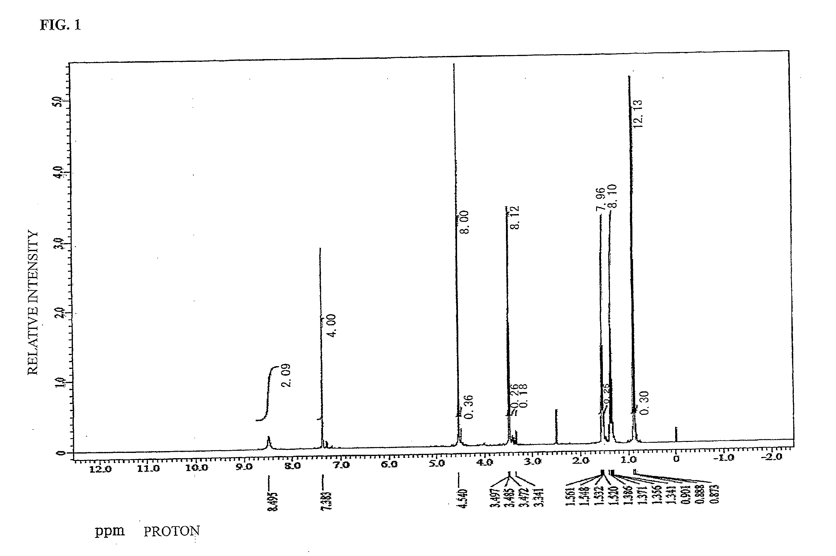
synthesis example 1
[0113]To a 100 mL recovery flask, TMOM-BP (20.00 g, 0.055 mol, manufactured by Honshu Chemical Industry Co., Ltd., Formula (4-23)) and PGME (propylene glycol monomethyl ether, 80.00 g) were charged and the mixture was stirred. The temperature of the mixture was raised until reflux was confirmed to dissolve the mixture and to start polymerization. 24 hours later, the reaction product was left to cool down to 30° C. Thereafter, TMOM-BP-PGME (a compound corresponding to Formula (3-4) was a main product and compounds of Formula (3-1), Formula (3-2), and Formula (3-3) were mixed in the compound of Formula (3-4)) in the PGME solution was obtained. As a result of identification of an existence ratio of the tetra-substituted compound of TMOM-BP-PGME carried out by GPC, the tetra-substituted compound existed in a ratio of 34 mol % in the whole TMOM-BP-PGME.
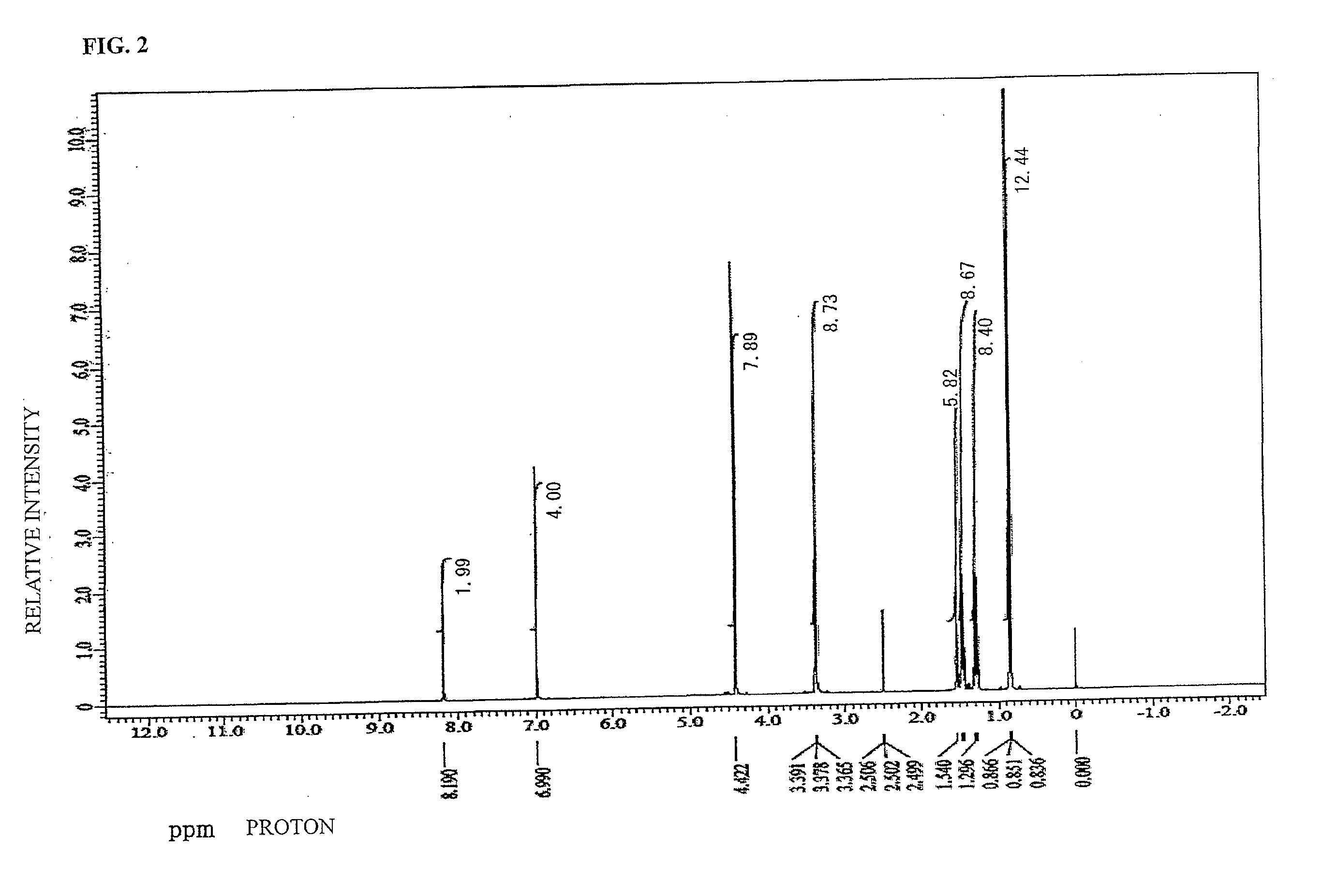
synthesis example 2
[0114]To a 200 mL recovery flask, TMOM-BP (5.00 g, 0.014 mol, manufactured by Honshu Chemical Industry Co., Ltd., Formula (4-23)), washed 15JWET (20.00 g, trade name Amberlist, manufactured by The Dow Chemical Company) as an ion-exchange resin for catalyst, and PGME (propylene glycol monomethyl ether, 75.00 g) were charged and the mixture was stirred. The temperature of the mixture was raised until reflux was confirmed to dissolve the mixture and to start polymerization. 48 hours later, the reaction product was left to cool down to 60° C. Thereafter, 15JWET was removed by filtration and the obtained precipitate was filtered to give a target product (a compound corresponding to Formula (3-4) was a main product and compounds of Formula (3-1), Formula (3-2), and Formula (3-3) were mixed in the compound of Formula (3-4), hereinafter abbreviated as TMOM-BP-PGME2).
[0115]As a result of identification of an existence ratio of the tetra-substituted compound of TMOM-BP-PGME2 carried out by GP...
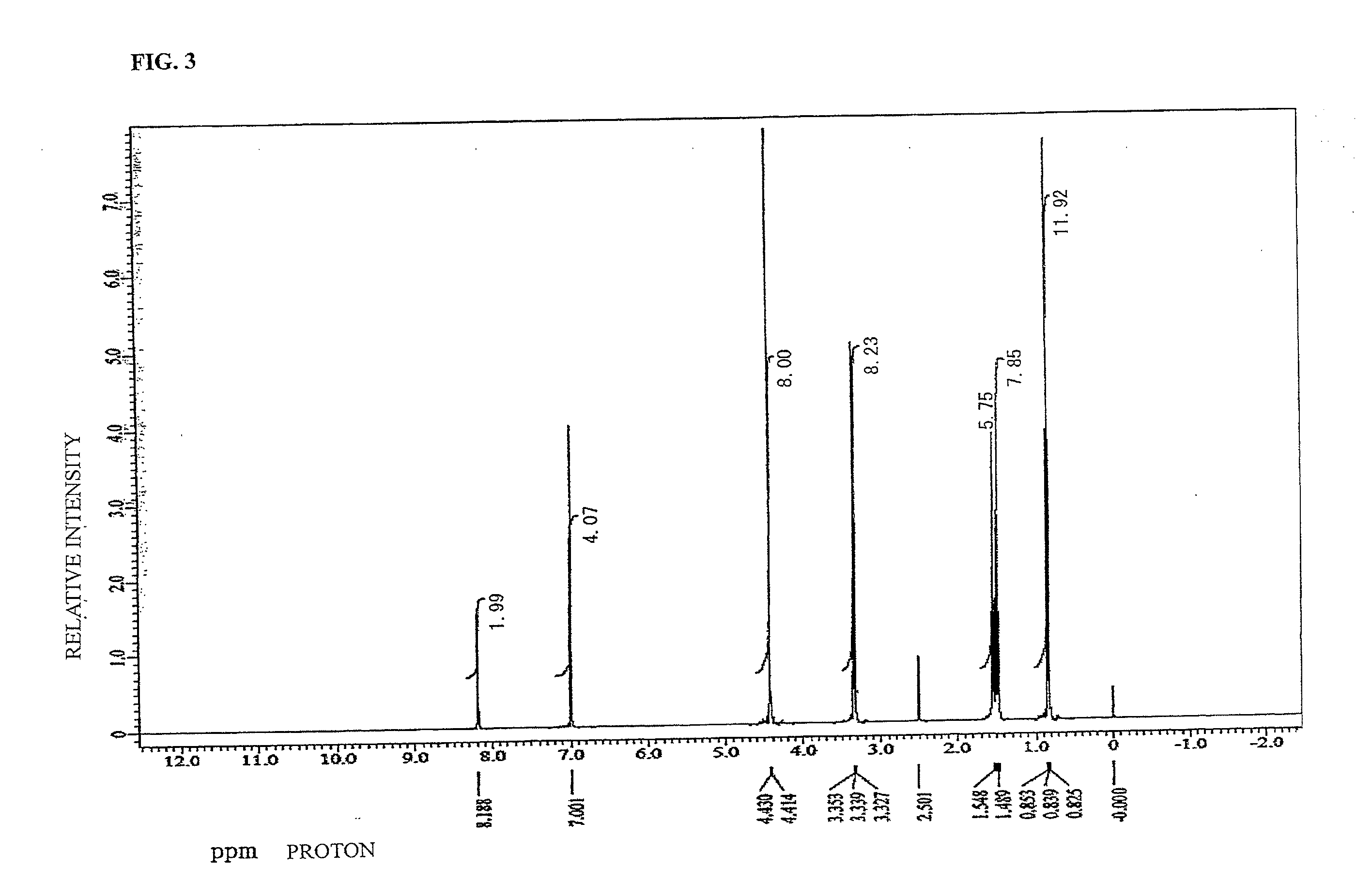
synthesis example 3
[0116]To a 200 mL four-necked flask, TMOM-BP (3.00 g, 0.008 mol, manufactured by Honshu Chemical Industry Co., Ltd., Formula (4-23)) and washed 15JWET (12.00 g, trade name Amberlist, manufactured by The Dow Chemical Company) as an ion-exchange resin for catalyst were added and butanol (60.00 g, manufactured by KANTO CHEMICAL CO., INC.) was charged. The mixture was stirred to start polymerization at 100° C. 48 hour later, the reaction product was left to cool down to 30° C. Thereafter, 15JWET was removed by filtration and the filtrate was concentrated at 30° C. under reduced pressure for 2 hours and dried to give 2.9 g of the target material (hereinafter abbreviated as TBOM-BP-BU; a compound corresponding to Formula (3-8) was a main product and compounds of Formula (3-5), Formula (3-6), and Formula (3-7) were mixed in the compound of Formula (3-8)).
[0117]Structure analysis was carried out with 1H-NMR to confirm that the target compound was obtained. The existence ratio of the tetra-s...
PUM
| Property | Measurement | Unit |
|---|---|---|
| temperature | aaaaa | aaaaa |
| thickness | aaaaa | aaaaa |
| wavelength | aaaaa | aaaaa |
Abstract
Description
Claims
Application Information