Method for makinga magnetic random access memory element with small dimension and high qulity

a random access memory and element technology, applied in the manufacture/treatment of galvano-magnetic devices, electrical apparatus, magnetic field-controlled resistors, etc., can solve the problems of increased information readout errors, decreased value changes, and still broken tunnel barriers, so as to improve device performance and magnetic stability, the effect of being more clean

Active Publication Date: 2016-06-09
SHANGHAI CIYU INFORMATION TECH
View PDF0 Cites 15 Cited by
  • Summary
  • Abstract
  • Description
  • Claims
  • Application Information

AI Technical Summary

Benefits of technology

This patent is about a method for making a small magnetic random access memory (MRAM) element by directly building a magnetic tunneling junction (MTJ) on a CMOS VIA. The method includes a process for flattening the interface of the bottom electrode during film deposition to ensure a smooth deposition of the MTJ layers. The invention has two process approaches, each with its own advantages. The first approach allows for smoother deposition and faster patterning, while the second approach allows for independent tuning of the bottom electrode process and further flattening of the surface. The technical effect of this patent is to make a small and efficient MRAM element with improved performance and magnetic stability.

Problems solved by technology

Even at a normal voltage operation, the tunnel barrier still could be broken if the tunnel layer is atomically rough from some points where the barrier gets thinner.
More, even when the tunnel barrier does not immediately break down, if recording operations are repeated, the element may still become nonfunctional such that the resistance value changes (decreases) and information readout errors increase, making the element un-recordable.
Furthermore, recording is not performed unless a sufficient voltage or sufficient spin current is applied.
Accordingly, problems with insufficient recording arise before possible tunnel barrier breaks down.
However, due to the presence of an electrical conducting material such as Cu, the top surface of the via is usually atomically rough, which, in return, will result in a rough MgO barrier (135) and a bad magnetic tunneling.
Unfortunately, such memory architecture will increase the dimension of the MRAM cell tremendously and make it impossible to increase memory density.

Method used


Image

  • Method for makinga magnetic random access memory element with small dimension and high qulity
  • Method for makinga magnetic random access memory element with small dimension and high qulity
  • Method for makinga magnetic random access memory element with small dimension and high qulity

Examples


embodiment one

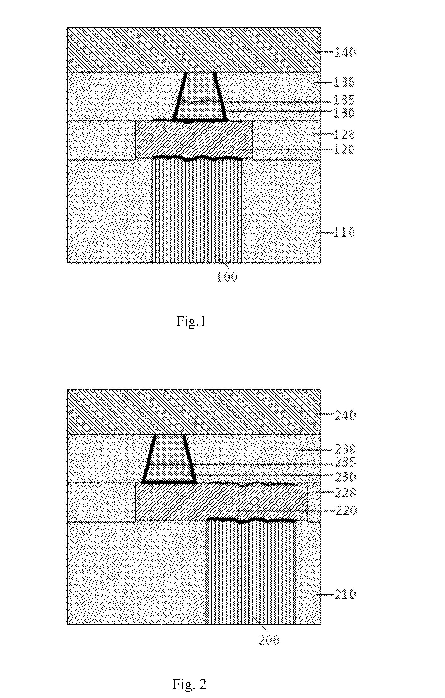
[0032]Following from the above BE deposition process, MTJ film deposition is continued without vacuum break. The deposition of MTJ film stack begins with seed layer, magnetic reference layer, magnetic tunneling oxide barrier layer, memory recording layer, capping layer and finally a hard mask layer. For pSTT-MRAM, the magnetic reference layer which is made of TbCoFe, CoX, or superlattice of [Co / X]n with X being Pt, Pd or Ni and n ranges from 5 to 20, has its uni-axial magnetic anisotropy in a direction perpendicular to a film surfaces with large coercivity (invariable). To further enhance its magnetic polarization invariability, the magnetic reference layer can be made as Y / Ru / CoFe, Y / Ru / CoFe / CoFeB with Y being TbCoFe or CoX and Ru with a thickness at its second (7-9 A) or first (3-4.5 A) oscillation peak. For in-plane STT-MRAM, the magnetic reference layer has tri-layer structure, either MnZ / Ru / CoFe or MnZ / Ru / CoFe / CoFeB with Z being either Pt, Pd or Ir. The tunnel oxide barrier lay...

embodiment two

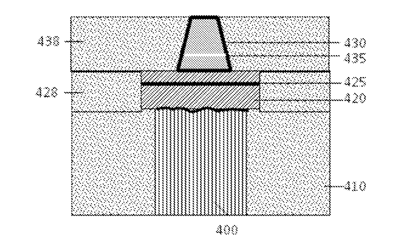
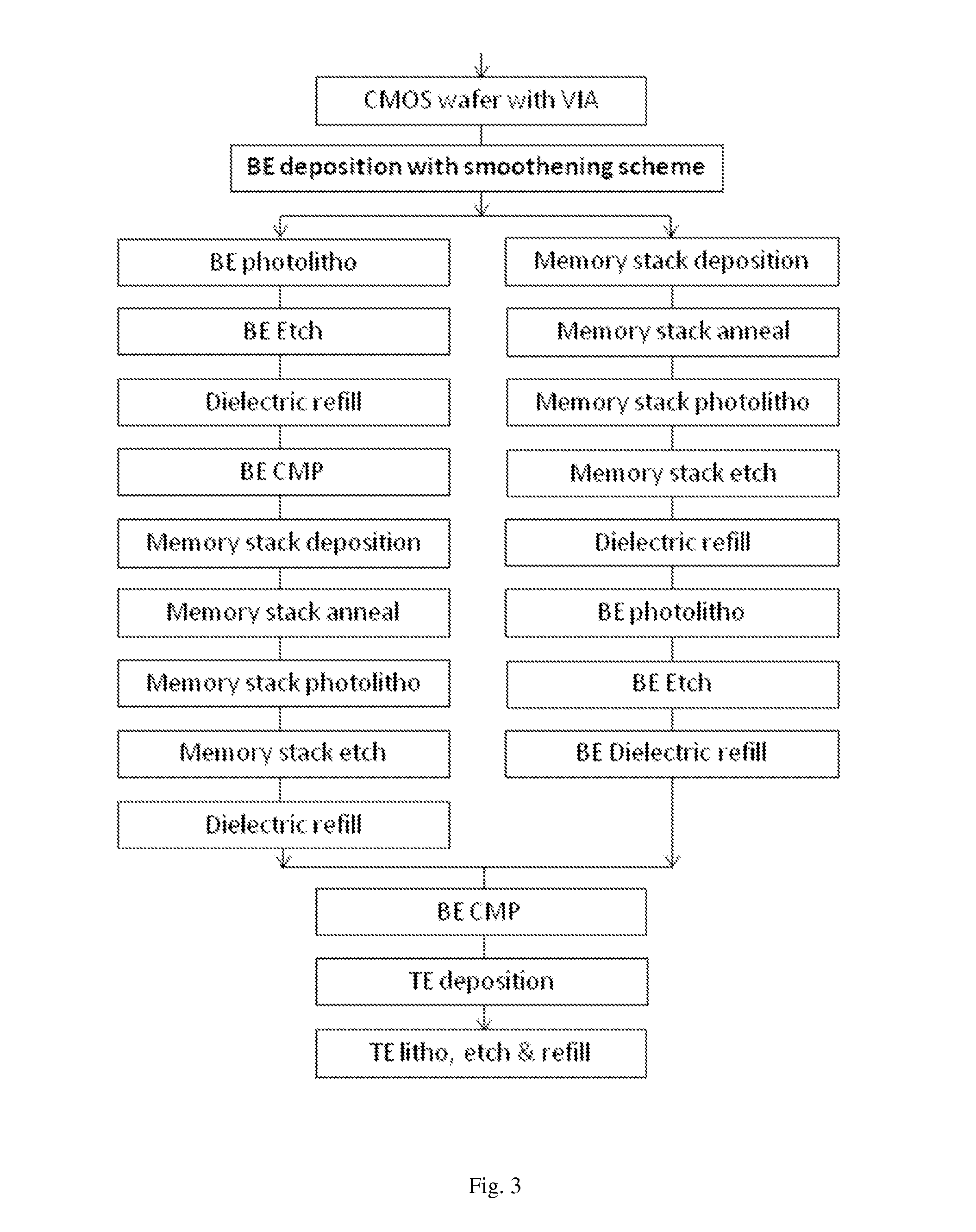
[0036]After the BE deposition and surface smoothening processes described in [0011], a complete BE is formed on CMOS VIAs (FIG. 5A). A photolithography patterning and etch are used to form an isolated BE. Then dielectric (SiO2 or SiN) refill (428) is used to cover the etched areas and an optional CMP is used to flatten the BE surface (FIG. 5B).

[0037]The wafer is moved in high vacuum physical deposition (PVD) chamber. The BE surface is sputtering cleaned, and then MTJ film stack is deposited on the patterned BE. The deposition of MTJ film stack (430) begin with seed layer, magnetic reference layer, magnetic tunneling oxide barrier layer (435), memory recording layer, capping layer and finally a hard mask layer. For pSTT-MRAM, the magnetic reference layer which is made of TbCoFe, CoX, CoX, CoX, or superlattice of [Co / X]n with X being Pt, Pd or Ni and n ranges from 5 to 30, has its uni-axial magnetic anisotropy in a direction perpendicular to a film surfaces with large coercivity (inva...


PUM


Abstract

This invention is about a method to make an MRAM element with small dimension, by building an MTJ as close as possible to an associated via connecting an associated circuitry in a semiconductor wafer. The invention provides a process scheme to flatten the interface of bottom electrode during film deposition, which ensures a good deposition of atomically smooth MTJ multilayer as close as possible to an associated via which otherwise might be atomically rough. The flattening scheme is first to deposit a thin amorphous conducting layer in the middle of BE deposition and immediately to bombard the amorphous layer by low energy ions to provide kinetic energy for surface atom diffusion to move from high point to low kinks. With such surface flattening scheme, not only the MRAM element can be made extremely small, but its device performance and magnetic stability can also be greatly improved.

Description

BACKGROUND OF THE INVENTION[0001]1. Field of the Invention[0002]This invention relates generally to a method for making magnetic random access memory (MRAM) element with small dimension and high quality for further making a complete high density and high yield MRAM.[0003]2. Description of the Related Art[0004]In recent years, MRAMs using the magnetoresistive effect of a ferromagnetic tunnel junctions or a magnetic tunnel junctions (MTJ) have been drawing increasing attention as the next-generation solid-state nonvolatile memories that can also cope with high-speed reading and writing. A ferromagnetic tunnel junction has a three-layer stack structure formed by stacking a recording layer having a changeable magnetization direction, an insulating tunnel barrier layer, and a fixed layer that is located on the opposite side from the recording layer and maintains a predetermined magnetization direction. Corresponding to the parallel and anti-parallel magnetic states between the recording ...

Claims


Application Information

Patent Timeline
IPC IPC(8): H01L43/12H01L43/08H01L43/02
CPCH01L43/12H01L43/08H01L43/02H10N50/80H10N50/10H10N50/01H10N50/85
Inventor XIAO, RONGFU
Owner SHANGHAI CIYU INFORMATION TECH
Why Eureka
Try Eureka