Methods for forming cobalt interconnects

a cobalt interconnect and cobalt technology, applied in the direction of contact devices, solid-state devices, chemical vapor deposition coatings, etc., can solve the problems of less reliable interconnects, negative consequences, other types of voids, etc., and achieve the effect of reducing overburden

Inactive Publication Date: 2016-10-20
APPLIED MATERIALS INC
View PDF7 Cites 35 Cited by
  • Summary
  • Abstract
  • Description
  • Claims
  • Application Information

AI Technical Summary

Benefits of technology

[0065]Annealing conditions for the ECD Co layer may be in a temperature range of 100 C to 400 C, and a pressure between 1 mTorr and 1 atm. In addition, a vacuum anneal is also within the scope of the present disclosure. The annealing environment may be hydrogen, a hydrogen/helium mix (e.g., 4% hydrogen, 96% helium), or a hydrogen/nitrogen mix (e.g., 4% hydrogen, 96% nitrogen). The time for the annealing process may be in the range of about 1 to about 60 minutes.
[0066]One advantageous effect of the methods described herein is single film filling the feature with no detectable interface between the electrochemically deposited film and the incoming “seed” film.
[0067]In the illustrated embodiment of FIGS. 1A-1F, the ECD Co process completely fills all features (small a...

Problems solved by technology

However, as feature dimensions on wafers decrease, negative consequences can come to bear.
For example, reduced-size features may result in less reliable interconnects.
A conventional copper fill to produce interconnects can result in voids, particularly in features having a size of less than 30 nm.
Other types of voids can also result from using conventional copper fill process in small features.
Such voids and other intrinsic properties of a deposit formed using conventional copper fill techniques can increase the resistance of the interconnect, thereby slowing down electrical performance of the device and reducing the reliability of the copper interconnect.
A further result of the ever-decreasing scaling down of interconnects is ...

Method used


Image

  • Methods for forming cobalt interconnects
  • Methods for forming cobalt interconnects
  • Methods for forming cobalt interconnects

Examples


example 1

[0111]The following is an exemplary flow path for a workpiece in processing equipment for forming cobalt interconnects. Exemplary systems for processing workpieces are provided in FIGS. 4-6.

[0112]Wafer carrier is loaded onto the system containing wafers prepared with a thin conformal conductive seed film (e.g., CVD Co).

[0113]Wafer is removed from the carrier in an ambient or low oxygen environment.

[0114](Optional) Wafer may be aligned to a common orientation (e.g., aligned to the notch).

[0115](Optional) Wafer processed with either a thermal or plasma pretreatment to reduce oxides and / or anneal. (This step may also be performed in upstream equipment.)

[0116]Automation system transfers the wafer to sequential processing station. This station may be in an ambient or low oxygen environment.

[0117]Wafer is processed in a deposition cell using a wet electrical contact allowing deposition at the contact area and to the edge of the wafer during processing.

[0118]Wafer is rinsed and dried in th...

example 2

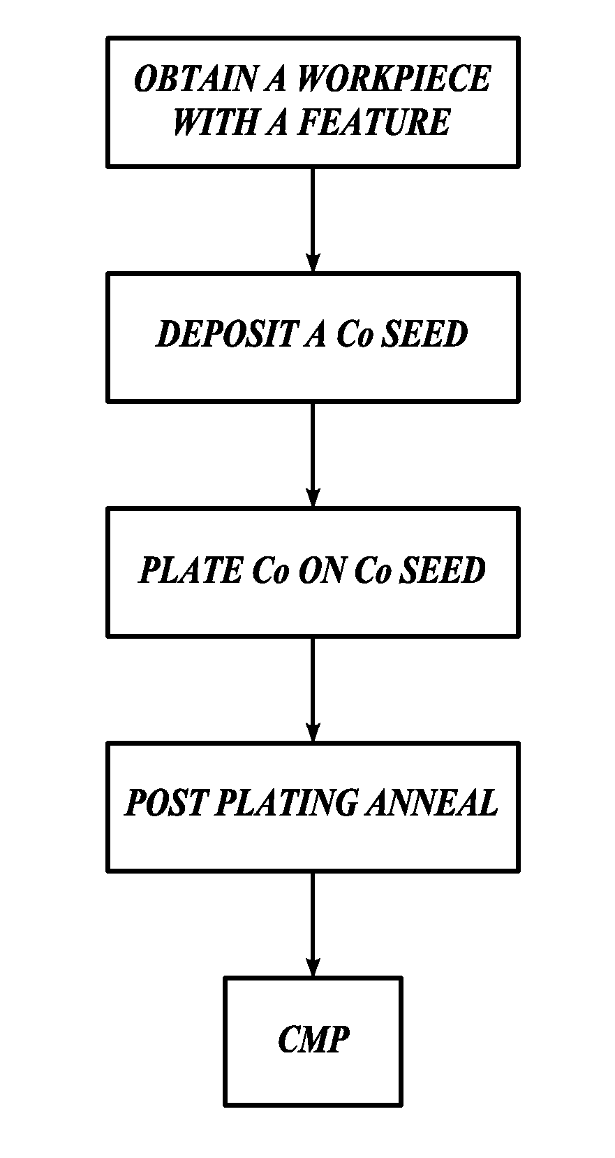
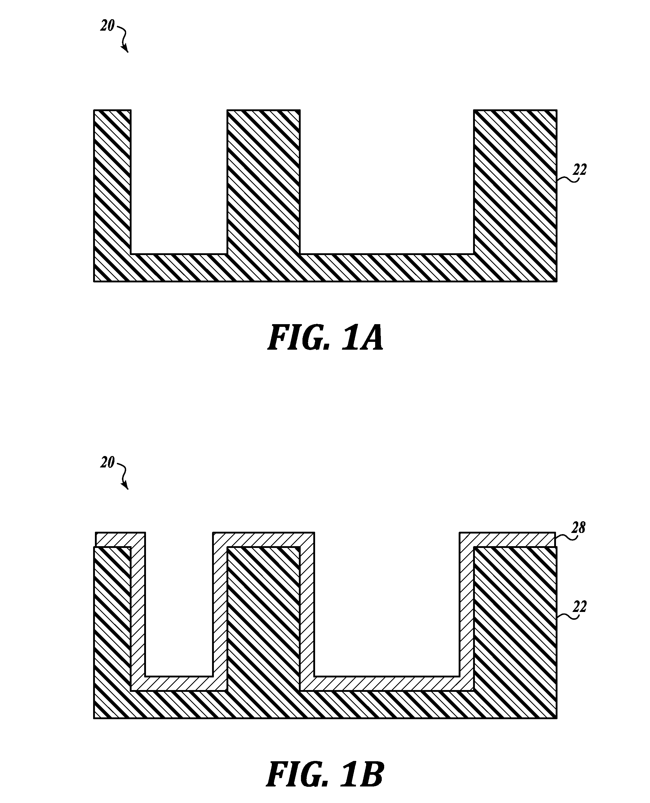
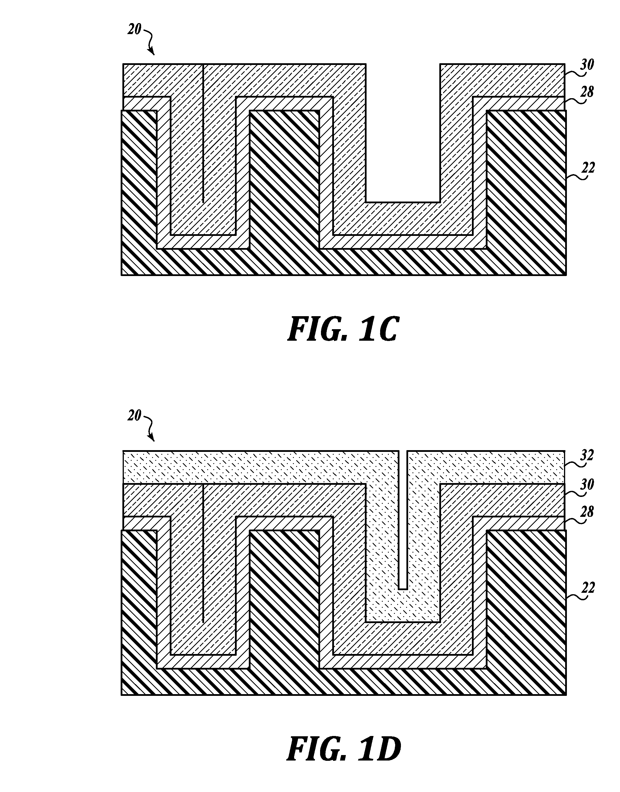
[0129]Referring to FIG. 11, an exemplary process for depositing a feature on a workpiece includes obtaining a workpiece with a feature, depositing a Co seed layer in the feature, electrochemically deposit a Co metallization layer on the Co seed layer, conducting a post-plating anneal, then subjecting the workpiece to CMP.

example 3

[0130]Referring to FIG. 12, an exemplary process is similar to the process in FIG. 11 and further includes a liner layer, such as an adhesion layer, deposited before the seed layer. The adhesion layer may be any suitable adhesion layer, such as a TiN or TaN layer.


PUM

PropertyMeasurementUnit
Nanoscale particle sizeaaaaaaaaaa
Temperatureaaaaaaaaaa
Dielectric polarization enthalpyaaaaaaaaaa

Abstract

A method for depositing metal in a feature on a workpiece includes forming a seed layer in a feature on a workpiece, wherein the seed layer includes a metal selected from the group consisting of cobalt and nickel; electrochemically depositing a first metallization layer on the seed layer, wherein electrochemically depositing the metallization layer includes using a plating electrolyte having a plating metal ion and a pH in the range of 6 to 13; and heat treating the workpiece after deposition of the first metallization layer.

Description

BACKGROUND[0001]The present disclosure relates to producing interconnects in semiconductor devices. Integrated circuits (IC) include various semiconductor devices formed within or on layers of dielectric material that overlay a substrate. Such devices which may be formed in or on the dielectric layers include MRS transistors, bipolar transistors, diodes, and diffused resistors. Other devices which may be formed in or on the dielectric material include thin film resistors and capacitors. Metal lines interconnect the semiconductor devices to power such devices and enable such devices to share and exchange information. Such interconnects extend horizontally between devices within a dielectric layer as well as vertically between dielectric layers. These metal lines are connected to each other by a series of interconnects. The electrical interconnects or metal lines are first patterned into the dielectric layers to form vertical and horizontal recessed features (vias and trenches) that a...

Claims


Application Information

Patent Timeline
IPC IPC(8): H05K3/18C25D5/34C21D1/26C25D3/12C22F1/10C21D9/00C25D7/12C25D5/50
CPCH05K3/181C25D7/123C25D5/34C25D5/50H05K3/188C22F1/10C21D9/0062C21D1/26C25D3/12H01L21/76879H01L23/53209H01L2221/1068H01L23/52H01L23/53238H01L21/76883H01L21/2885H01L21/76861H01L21/76862H01L21/76873H01L21/76877H01L21/76882C25D3/38C25D5/10C23C18/1653C25D17/005C25D21/12C23C14/16C23C16/06C23C18/32H01L21/28556
Inventor SHAVIV, ROEYLAM, JOHN W.BOCHMAN, TIMOTHYTSENG, JENNIFER MENG CHU
Owner APPLIED MATERIALS INC
Why Eureka
Try Eureka