

Processing of thin film organic ferroelectric materials using pulsed electromagnetic radiation
a technology of electromagnetic radiation and organic ferroelectric materials, applied in the direction of piezoelectric/electrostrictive device details, instruments, device details, etc., can solve the problems of low relative speed, long write cycles (ms), and relatively low cost of rom, so as to reduce overall cost, time to make, and promote crystallization of precursor materials
- Summary
- Abstract
- Description
- Claims
- Application Information
AI Technical Summary
Benefits of technology
Problems solved by technology
Method used
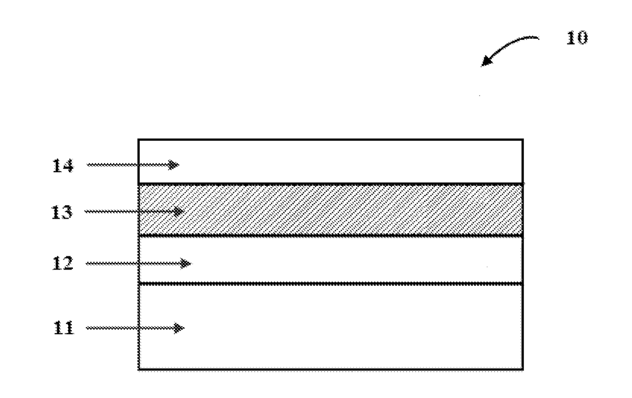
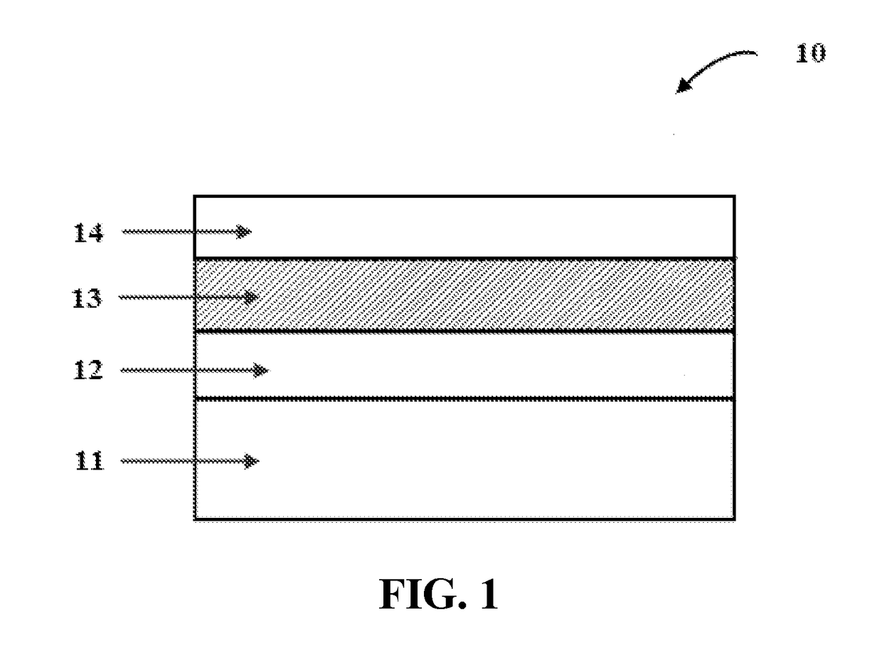
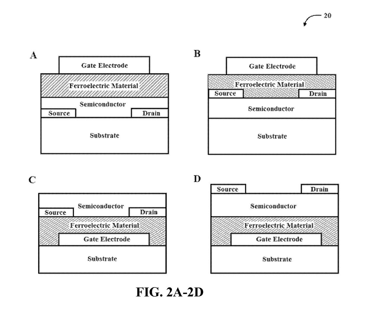
Image

Examples
example 1
Preparation of Ferroelectric Precursor Material
[0072]5.1 wt. % polyvinylidene fluoride (PVDF) was solubilized in dimethylformamide (DMF) to obtain a solution. The solution was spin-coated (3000 rpm for 60 sec.) onto a platinum-coated silicon wafer to obtain a thin film of approximately 190 nm. The films were spun, stored inside a standard “gel-pak”, and exposed to the radiation 6 days later.
example 2
Processing of the Ferroelectric Precursor Material into Ferroelectric Material Having Ferroelectric Hysteresis Properties
[0073]Following the casting of the platinum-coated silicon wafer supported PVDF thin film solution, and without any form of heating, the thin film solution was directly exposed to light irradiation from a PulseForge 1300 photonic curing tool, supplied by Novacentrix (Austin, Tex., USA). The following parameters were used via Novacentrix's Simpulse® software, which is used in conjunction with the PulseForge tool:[0074](1) Pulse radiant energy approximately 2-4 J / cm2.[0075](2) Pulse Depth approximately 200 nm.[0076](3) Output Light Spectrum 200 to 1000 nm.[0077](4) Pulse Length: None; Short (about 200 μs), Medium (about 400 μs), and Long (about 800 μs).[0078](5) Pulse Frequency: Adjusted by the Simpulse® software from a single pulse to 1 Hz to maintain the pulse temperature and pulse length delivered to the PVDF thin film solution.
[0079]For comparative data, the tes...
example 3
Ferroelectric Hysteresis Properties of Produced Ferroelectric Material
[0080]Following photonic exposure using the PulseForge tool, Au electrodes were evaporated using a shadow mask to cover the entire top surface of the film for ferroelectric characterization. FIG. 7 provides the results of these tests. In particular, at least 4 devices from each region were tested. As evident in FIG. 7, the best ferroelectric hysteresis loops were obtained over the sample area exposed to the longest pulse length (Region 4). This area on the sample was specifically able to withstand high fields (>250 MV / m) without showing top electrode explosions typically seen with as-spun samples. The memory device exhibits saturated ferroelectric polarization hysteresis upon electroforming of the device at electric fields of ˜250 MV / m, showing a remnant polarization of about 5 μC / cm2 and coercive field of about 110 MV / m at 10 Hz. This is in line with the best reported polarization hysteresis loops for PVDF. Mediu...
PUM
| Property | Measurement | Unit |
|---|---|---|
| Time | aaaaa | aaaaa |
| Time | aaaaa | aaaaa |
| Polarity | aaaaa | aaaaa |
Abstract
Description
Claims
Application Information