Crystalline semiconductor film, plate-like body and semiconductor device

a technology of crystalline semiconductor and film, applied in the direction of coating, transistor, chemical vapor deposition coating, etc., can solve the problems of inability to maintain sufficient withstand voltage, difficult to be used for a semiconductor device, many constraints to be applied, etc., to achieve excellent withstand voltage, inhibit leakage current, and excellent semiconductor properties

Active Publication Date: 2017-07-13
FLOSFIA
View PDF11 Cites 36 Cited by
  • Summary
  • Abstract
  • Description
  • Claims
  • Application Information

AI Technical Summary

Benefits of technology

[0022]The crystalline semiconductor film and the sheet like object of the present invention are excellent in semiconductor properties and the semiconductor device of the present invention has inhibited leakage current and is excellent in withstand voltage and heat dissipation.

Problems solved by technology

The thin film in PTL 1 is, however, not capable of maintaining sufficient withstand voltage.
This film also contains many carbon impurities and has unsatisfactory semiconductor properties including conductivity, so that the film is difficult to be used for a semiconductor device.
The semiconductor element in PTL 2, however, has many constraints to be applied to a semiconductor element due to α-Al2O3 being an insulator and the crystal quality with some problems.
The p type α-Al2O3 itself is accordingly difficult to be achieved, and in reality, the semiconductor element in PTL 2 itself is difficult to be achieved.
The description, however, mentions that the crystal grows up to a film thickness of 100 nm at a temperature of 450° C. or less while the quality of the crystal becomes poor with a film thickness more than that and a film with a film thickness of 1 μm or more cannot be obtained.
In addition, all films obtained in the methods of PTLs 3 to 6 were not able to be peeled off from the substrate in reality.

Method used


Image

  • Crystalline semiconductor film, plate-like body and semiconductor device
  • Crystalline semiconductor film, plate-like body and semiconductor device
  • Crystalline semiconductor film, plate-like body and semiconductor device

Examples


example 1

1. Film Formation Apparatus

[0132]With reference to FIG. 18, a mist CVD apparatus 19 used in the present Example is described. The mist CVD apparatus 19 was provided with a susceptor 21 to place a substrate 20, carrier gas supply means 22 to supply a carrier gas, a flow regulating valve 23 to regulate a flow rate of the carrier gas discharged from the carrier gas supply means 22, a mist generator 24 to store a raw-material solution 24a, a container 25 to keep water 25a, an ultrasonic vibration transducer 26 mounted at a bottom of the container 25, a supply pipe 27 of a quartz pipe with an inner diameter of 40 mm, and a heater 28 placed surrounding the supply pipe 27. The susceptor 21 was made from quartz and had a surface to place the substrate 20 inclined from the horizontal plane. Both the supply pipe 27 and the susceptor 21 made from quartz inhibit mixing of impurities derived from the apparatus into the film formed on the substrate 20.

[0133]As the susceptor 21, the susceptor 51 i...

example 2

[0141]Respective raw-material solutions of gallium bromide and germanium oxide were prepared at an atomic ratio of germanium to gallium of 1E-7, 1E-6, 8E-5, 4E-4, 2E-3, 1E-2, 2E-1, and 8E-1. At this point, a 48% hydrobromic acid solution was contained at a volume ratio of 10%. Films were formed in the film formation conditions same as those in Example 1 for quantitative analysis of the concentration of impurities using SIMS, the type of incident ion of oxygen, and output of 3 kV and 200 nA. The results are illustrated in FIG. 21. As illustrated in FIG. 21, it was found that a dopant content ratio in the liquid and a doping amount in the crystal film have a correlation and adjustment of the dopant content ratio in the liquid facilitates control of the doping concentration in the film to be formed.

example 3

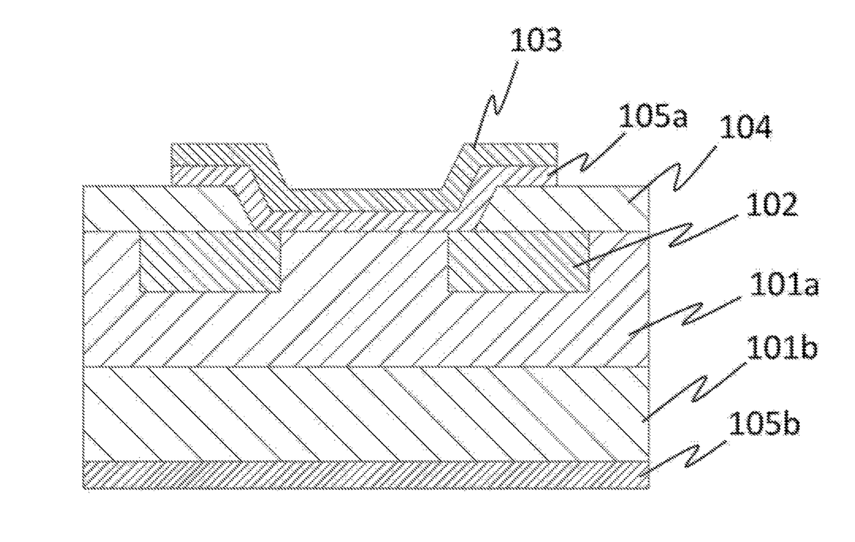
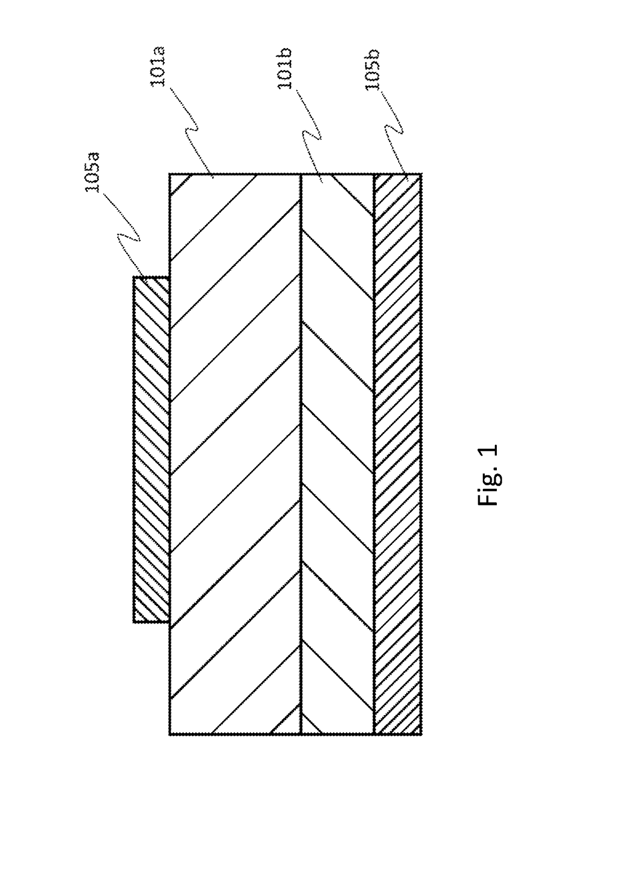
[0142]In the same manner as in Condition 1 other than changing the concentration of germanium oxide to 1.0×10⁻³ mol / L instead of 5.0×10⁻³ mol / L, a germanium doped α-Ga2O3 film was formed on the c-plane sapphire substrate as the n+ semiconductor layer. On the film thus formed, an undoped α-Ga2O3 film was then formed as the n− semiconductor layer. The n− semiconductor layer was formed in the same manner as above other than doping was not performed. The crystalline semiconductor film thus obtained had a film thickness of 7.6 μm and the film formation time was 180 minutes. Then, as illustrated in FIG. 22, part of the n− semiconductor layer 101a was etched, followed by providing the ohmic electrode 105b of Ti on the n+ semiconductor layer 101b and the Schottky electrode 105a on the n− semiconductor layer 101a by sputtering to fabricate an SBD.

[0143]The SBD thus obtained was subjected to SIMS analysis (Cs, 3 kV, 200 nA, Ap 16%, Raster 400). The results are illustrated in FIG. 23. As clear...


PUM

PropertyMeasurementUnit
thicknessaaaaaaaaaa
thicknessaaaaaaaaaa
thicknessaaaaaaaaaa

Abstract

A semiconductor film, a sheet like object, and a semiconductor device are provided that have inhibited semiconductor properties, particularly leakage current, and excellent withstand voltage and heat dissipation. A crystalline semiconductor film or a sheet like object includes a corundum structured oxide semiconductor as a major component, wherein the film has a film thickness of 1 μm or more. Particularly, the semiconductor film or the object includes a semiconductor component of oxide of one or more selected from gallium, indium, and aluminum as a major component. A semiconductor device has a semiconductor structure including the semiconductor film or the object.

Description

TECHNICAL FIELD[0001]The present invention relates to a crystalline semiconductor film and a sheet like object that are useful for a semiconductor device and a semiconductor device using the crystalline semiconductor film or the sheet like object.BACKGROUND ART[0002]As a switching device of the next generation achieving high withstand voltage, low losses, and high temperature resistance, semiconductor devices using gallium oxide (Ga2O3) with a large band gap attract attention and are expected to be applied to power semiconductor devices, such as an inverter. According to NPL 1, such gallium oxide has a band gap that may be controlled by forming mixed crystal with indium or aluminum singly or in combination. Among all, InAlGaO-based semiconductors represented by InxAlyGazO3 (0≦X′≦2, 0≦Y′≦2, 0≦Z′≦2, X′+Y′+Z′=1.5 to 2.5) are extremely attractive materials.[0003]PTL 1 describes a highly crystalline conductive α-Ga2O3 thin film with an added dopant (tetravalent tin). The thin film in PTL...

Claims


Application Information

Patent Timeline
Patent Type & Authority Applications(United States)
IPC IPC(8): H01L29/24H01L29/778H01L29/808H01L29/772H01L29/739H01L33/26H01L29/78H01L29/66H01L33/00H01L29/812H01L21/02C23C16/448C23C16/44C23C16/40H01L29/872
CPCH01L29/24C23C16/40H01L29/778H01L29/8083H01L29/7722H01L29/7395H01L33/26H01L29/78H01L29/66969H01L33/005H01L29/8122H01L21/02565H01L21/0262C23C16/4481C23C16/4415H01L29/872H01L29/812H01L21/0242H01L21/02628H01L29/7787H01L29/8725H01L29/04H01L33/44H01L29/7827H01L21/02576H01L21/02579H01L21/0257H01L21/02414H01L21/20H01L27/098H01L29/12H01L29/47H01L29/739H01L29/808H01L21/02573
Inventor HITORA, TOSHIMIODA, MASAYATAKATSUKA, AKIO
Owner FLOSFIA
Why Eureka
Try Eureka