

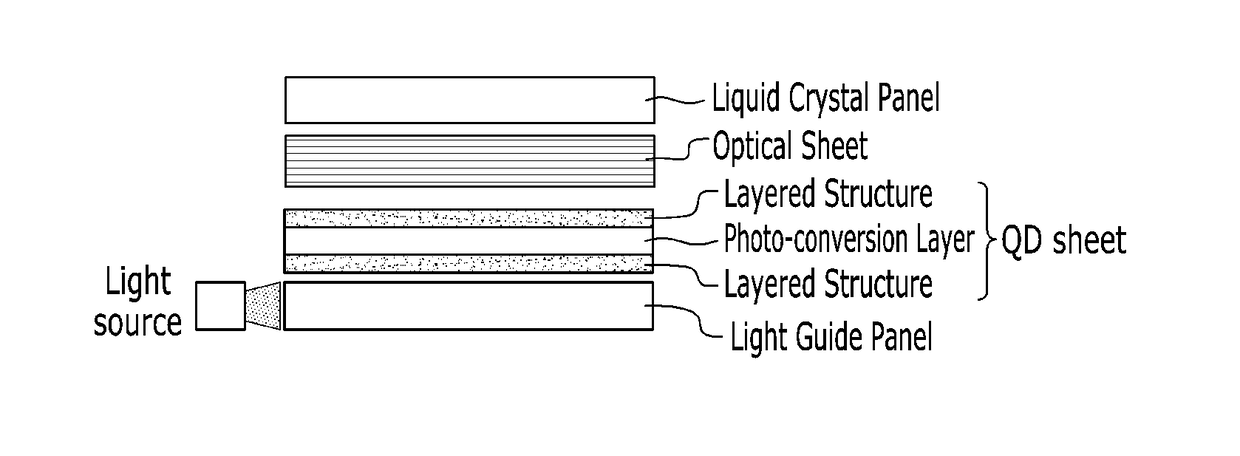
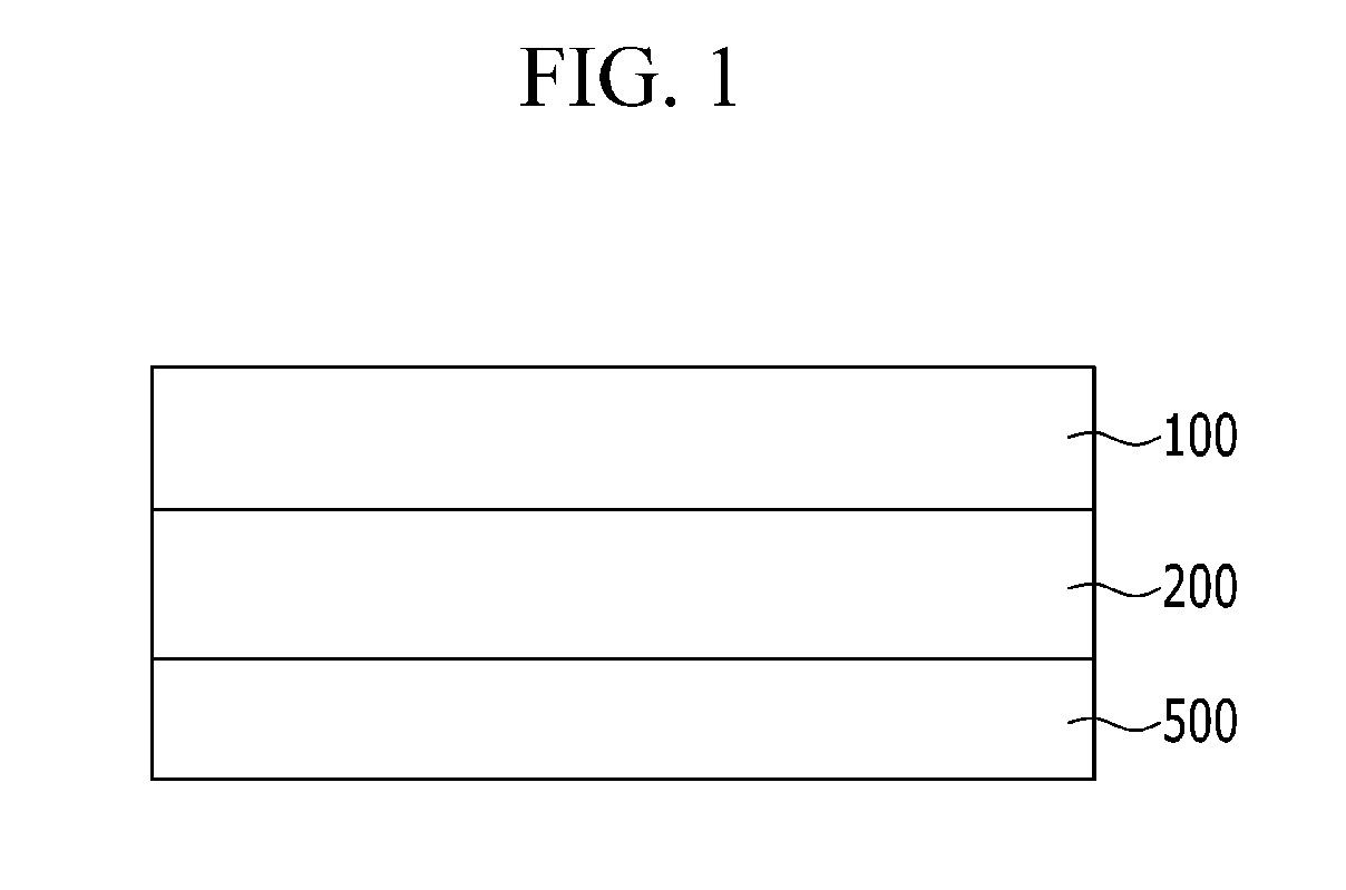
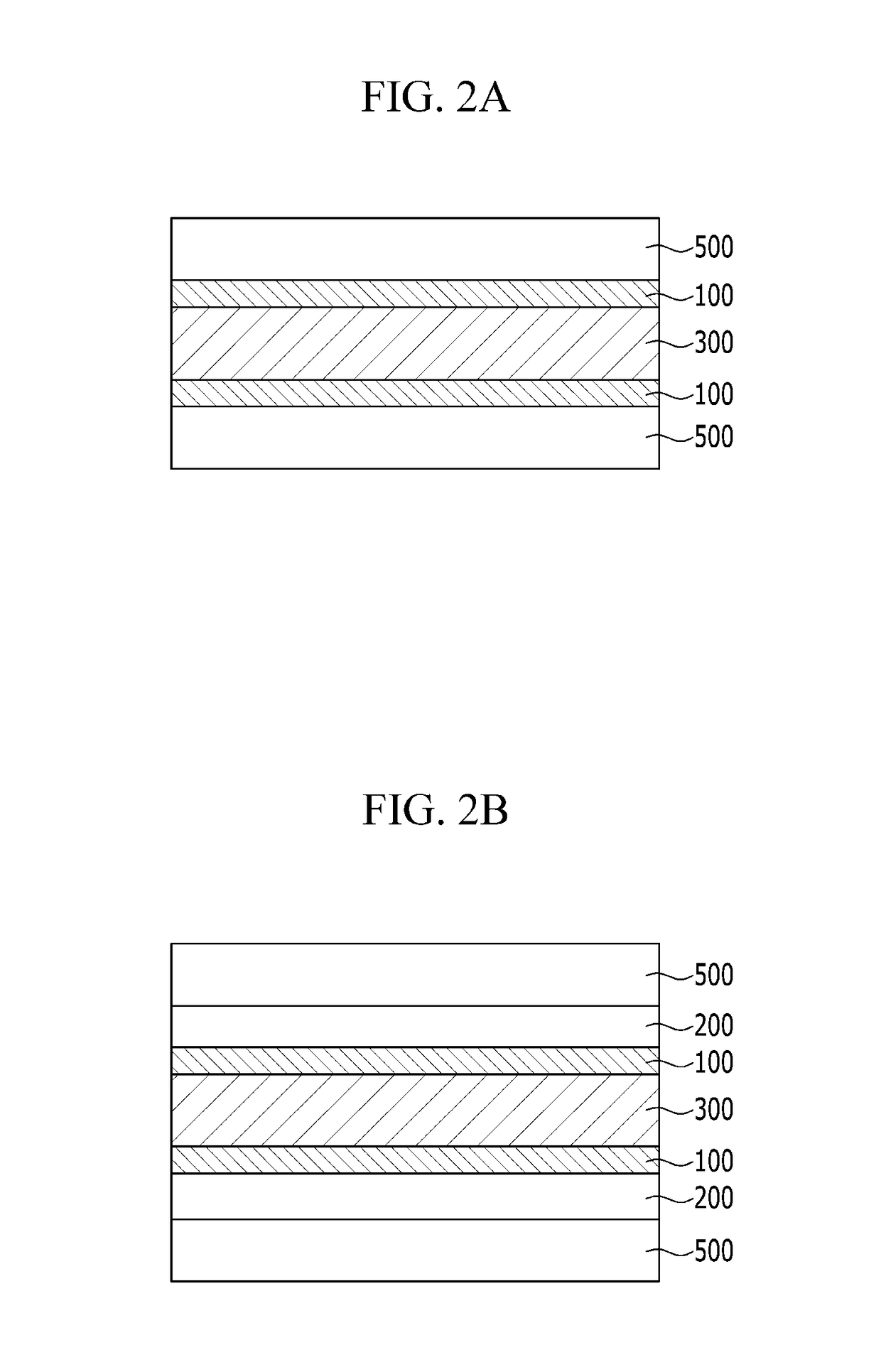
Layered structures and quantum dot sheets and electronic devices including the same
a quantum dot and layer structure technology, applied in the field of layers and quantum dot sheets and electronic devices including the same, can solve the problems of economic and technological inferior barrier coatings, reduce performance under harsh conditions, etc., and achieve the effect of improving the reliability of barrier coatings and enhancing stability
- Summary
- Abstract
- Description
- Claims
- Application Information
AI Technical Summary
Benefits of technology
Problems solved by technology
Method used
Image

Examples
reference example 1
Semiconductor Nanocrystals
[0211](1) 0.2 millimoles (mmol) of indium acetate, 0.6 mmol of palmitic acid, and 10 milliliters (mL) of 1-octadecene are placed in a flask, subjected to a vacuum state at 120° C. for one hour, and then, heated to 280° C. after the atmosphere in the flask is exchanged with N2. Then, a mixed solution of 0.1 mmol of tris(trimethylsilyl)phosphine (TMS3P) and 0.5 mL of trioctylphosphine (TOP) is quickly injected, and the reaction proceeds for 20 minutes. The reaction mixture then is rapidly cooled and acetone is added thereto to produce nanocrystals, which are then separated by centrifugation and dispersed in toluene. The first absorption maximum in UV-VIS spectrum of the InP core nanocrystals thus prepared is in the range of 420 to 600 nm.
[0212]0.3 mmol (0.056 grams, g) of zinc acetate, 0.6 mmol (0.189 g) of oleic acid, and 10 mL of trioctylamine are placed in a flask, subjected to a vacuum state at 120° C. for 10 minutes, and then heated to 220° C. after the ...
reference example 2
mposition for a Photoconversion Layer
[0214]30 parts by weight of lauryl methacrylate (as a monomer), 36 parts by weight of tricyclodecane dimethanol diacrylate (as a monomer), 4 parts by weight of trimethylol propane triacrylate (as a monomer), and 20 parts by weight of epoxy diacrylate oligomer (from Sartomer) (as an oligomer), 1 parts by weight of 1-hydroxy-cyclohexyl-phenyl-ketone, and 1 parts by weight of 2,4,6-trimethylbenzoyl-diphenyl-phosphine oxide are mixed to prepare a mixture. The mixture is defoamed under vacuum.
[0215]Semiconductor nanocrystals are centrifuged once in the same manner as Reference Example 1. The resulting toluene dispersion of the semiconductor nanocrystals is mixed with an excess amount of ethanol and then centrifuged. The semiconductor nanocrystals thus separated are dispersed in 0.15 g of lauryl methacrylate (as a monomer), and then added to 1.35 g of the prepared monomer-oligomer mixture and vortexed to prepare a quantum dot composition.
experimental example 1
Properties Depending on a Thiol Structure I
[0216][1] pentaerythritol tetrakis(3-mercaptopropionate) (THIOCURE PETMP, manufacturer: Bruno Bock Chem., hereinafter 4T) and 1,3,5-triallyl-1,3,5-triazine-2,4,6(1H,3H,5H)-trione (TAIC, manufacturer: Nippon Kasei Chemical, hereinafter TTT are mixed at a weight ratio of 60 / 40=4T / TTT. Irgacure TPO (Manufacturer: BASF) is added thereto in an amount of 1 wt % based on a total weight of the mixture of 4T / TTT to form a composition for the formation of the first layer.
[0217]The composition for the formation of the 1st layer, thus obtained, is bar-coated on a 50 micrometer (μm)-thick PET base film with a wire bar and then is exposed to ultraviolet (UV) radiation (light intensity: 150 milliwatts per square centimeter, mW / cm2) for 10 seconds to obtain a layered structure including a first layer having a predetermined thickness set forth in Table 1 and a PET substrate. The same procedure is repeated to prepare the same layered structure as above.
[0218...
PUM
| Property | Measurement | Unit |
|---|---|---|
| thickness | aaaaa | aaaaa |
| thickness | aaaaa | aaaaa |
| temperature | aaaaa | aaaaa |
Abstract
Description
Claims
Application Information