

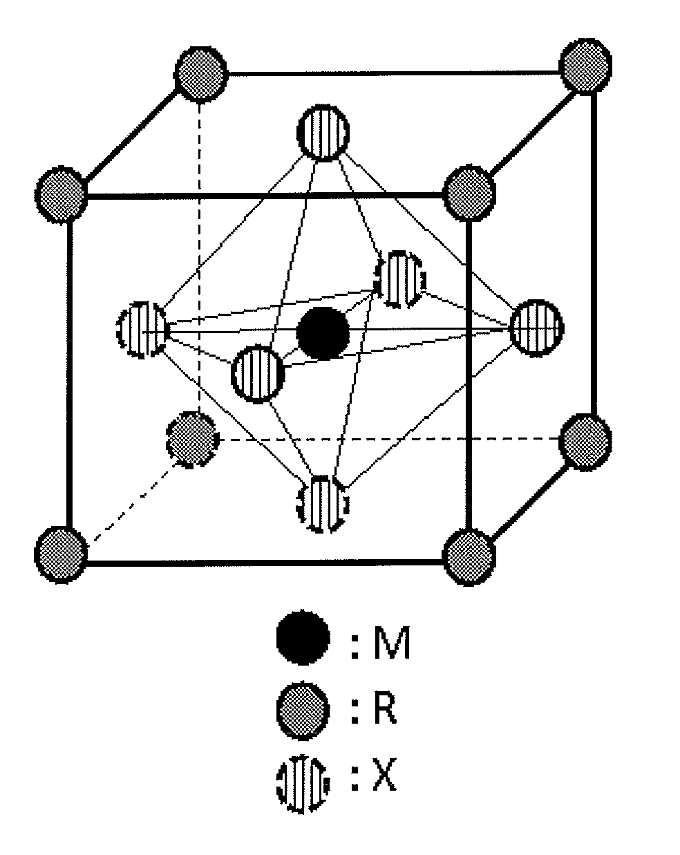
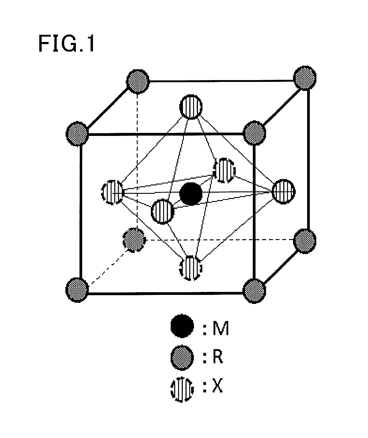
Solar cell and solar cell manufacturing method
a solar cell and manufacturing method technology, applied in the field of solar cells, can solve the problems of limited application of organic solar cells, and achieve the effect of reducing photodegradation and reducing photoelectric conversion efficiency
- Summary
- Abstract
- Description
- Claims
- Application Information
AI Technical Summary
Benefits of technology
Problems solved by technology
Method used
Image

Examples
example 1
(1) Preparation of Titanium-Containing Coating Liquid
[0099]Ten millimoles of titanium powder was precisely weighed and put in a beaker. To the beaker were further added 40 g of aqueous hydrogen peroxide and 10 g of aqueous ammonia. The mixture was cooled with water for two hours before adding 30 mmol of L-lactic acid. The mixture was then heated on a hot plate set at 80° C. for one day. To the mixture was then added 10 mL of distilled water, thus a titanium-containing coating liquid was prepared.
(2) Preparation of Solar Cell
[0100]A FTO film having a thickness of 1,000 nm as an electrode (cathode) was formed on a glass substrate, ultrasonically washed with pure water, acetone, and methanol each for 10 minutes in the stated order, and then dried.
[0101]The titanium-containing coating liquid was applied at 1,500 rpm by the spin coating method and then fired in air at 550° C. for 10 minutes to form a thin film-shaped electron transport layer. Onto the thin film-shaped electron transport ...
examples 2 to 14
[0108]A solar cell was obtained in the same manner as in Example 1 except that instead of 0.01 M of copper chloride of Example 1, the compound and the amount shown in Table 1 were employed in the preparation of the solution for organic-inorganic perovskite compound formation, and that the material of the hole transport layer was changed to that shown in Table 1. The properties of the organic-inorganic perovskite compound including the degree of crystallinity and carrier density were measured in the same manner as in Example 1.
examples 15 and 16
[0109]On the porous electron transport layer of Example 1, CH3NH3I and PbI2 were dissolved at a mole ratio of 1:1 into N,N-dimethylformamide (DMF) as a solvent to achieve a Pb concentration of 1 M, thereby preparing a solution for organic-inorganic perovskite compound formation. In order to add strontium or titanium, strontium chloride or titanium iodide as an additive was dissolved into the thus prepared solution to a concentration of 0.01 M. The resulting solution was applied onto the above porous electron transport layer by the spin coating method to form a film. Further, 1 wt % solution of poly(4-butylphenyl-diphenyl-amine) (available from 1-Material) in chlorobenzene was applied onto the organic-inorganic perovskite compound part by the spin coating method to a thickness of 50 nm to form a hole transport layer, whereby a photoelectric conversion layer was formed. A gold film having a thickness of 100 nm was formed as a counter electrode (anode) on the photoelectric conversion l...
PUM
 Abstract
Description
Claims
Application Information