Photoelectric conversion device and imaging unit

a conversion device and imaging unit technology, applied in the manufacture of final products, basic electric elements, radio-controlled devices, etc., can solve the problems of reducing the manufacturing yield, achieve high carrier mobility, improve device characteristics, and improve stereoregularity p3ht

Inactive Publication Date: 2018-12-20
SONY CORP
View PDF2 Cites 5 Cited by
  • Summary
  • Abstract
  • Description
  • Claims
  • Application Information

AI Technical Summary

Benefits of technology

[0011]PTL 1 and NPL 3 described above report that the higher a stereoregularity ratio P3HT has, the higher carrier mobility is achieved; therefore, P3HT is preferable as a material of a photoelectric conversion device. However, P3HT having a high stereoregularity ratio has high crystallinity; therefore, film surface flatness is low, thereby causing an issue that manufacturing yields are decreased.
[0012]It is desirable to provide a photoelectric conversion device and an imaging unit that have high quantum efficiency and allow for an improvement in manufacturing yields.
[0015]In the photoelectric conversion device according to the embodiment of the present disclosure and the imaging unit according to the embodiment of the present disclosure, the photoelectric conversion layer is formed with use of the first organic semiconductor having head-to-tail coupling stereoregularity of 95% or more represented by the foregoing formula (1) and the second organic semiconductor having head-to-tail coupling stereoregularity of 75% or more but less than 95% also represented by the foregoing formula (1). Accordingly, crystallinity of the first organic semiconductor material is suppressed, and the photoelectric conversion layer having a flat surface is achieved. Moreover, a ratio of Face-on orientation of a polymer including a molecular structure represented by the foregoing formula (1) in the photoelectric conversion layer is enhanced.
[0016]According to the photoelectric conversion device of the embodiment of the present disclosure and the imaging unit of the embodiment of the present disclosure, the photoelectric conversion layer is configured with use of the first organic semiconductor having head-to-tail coupling stereoregularity of 95% or more represented by the foregoing formula (1) and the second organic semiconductor having head-to-tail coupling stereoregularity of 75% or more but less than 95% also represented by the foregoing formula (1), which makes it possible to flatten the surface of the photoelectric conversion layer. Moreover, the ratio of Face-on orientation of a polymer including the molecular structure represented by the foregoing formula (1) in the photoelectric conversion layer is enhanced, which makes it possible to improve carrier mobility. This makes it possible to provide a photoelectric conversion device having improved manufacturing yields and improved quantum efficiency and an imaging unit including the same. It is to be noted that effects described herein are not necessarily limited, and any of effects described in the present disclosure may be included.

Problems solved by technology

However, P3HT having a high stereoregularity ratio has high crystallinity; therefore, film surface flatness is low, thereby causing an issue that manufacturing yields are decreased.

Method used


Image

  • Photoelectric conversion device and imaging unit
  • Photoelectric conversion device and imaging unit
  • Photoelectric conversion device and imaging unit

Examples


embodiment

1. EMBODIMENT

(1-1. Basic Configuration)

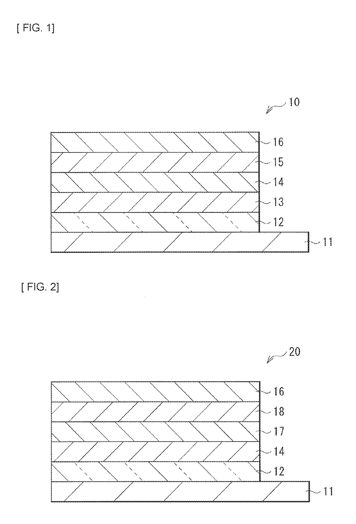
[0036]FIG. 1 illustrates an example of a cross-sectional configuration of a photoelectric conversion device (a photoelectric conversion device 10) according to a first embodiment of the present disclosure. The photoelectric conversion device 10 is applied to, for example, a solar battery (a solar battery 1, refer to FIG. 6). The photoelectric conversion device 10 has a configuration in which a transparent electrode 12, a hole transport layer 13, an organic photoelectric conversion layer 14, an electron transport layer 15, and a counter electrode 16 are stacked in this order on a substrate 11. In the photoelectric conversion device 10 according to the present embodiment, the organic photoelectric conversion layer 14 is formed including an organic semiconductor material (a first organic semiconductor material) having head (Head)-to-tail (Tail) coupling stereoregularity of 95% or more and an organic semiconductor material (a second organic semicon...

second embodiment

2. SECOND EMBODIMENT

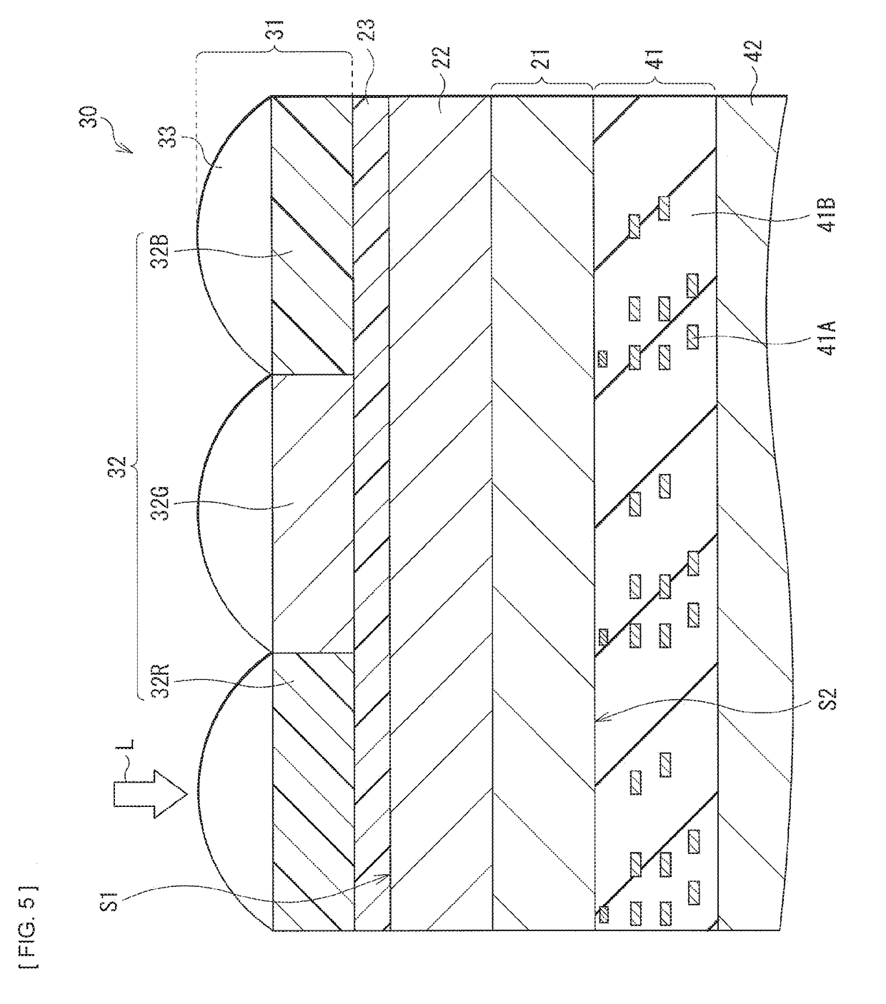
[0077]FIG. 5 illustrates a cross-sectional configuration of a photoelectric conversion device (an imaging device 30) according to a second embodiment of the present disclosure. The imaging device 30 configures one pixel (for example, a pixel P) in, for example, an imaging unit (for example, an imaging unit 2) such as a Bayer arrangement type CCD image sensor or CMOS image sensor (both refer to FIG. 7). This imaging device 30 is of a back-side illumination type, and has a configuration in which a light concentration section 31 and a photoelectric converter 22 are provided on a side on which a light incident surface is located of a semiconductor substrate 21, and a multilayer wiring layer 41 is provided on a surface (a surface S2) opposite to a light reception surface (a surface S1).

[0078]In the imaging device 30, for example, the photoelectric converter 22 is provided on, for example, the semiconductor substrate 21. The photoelectric converter 22 according to the ...

application examples

3. APPLICATION EXAMPLES

Application Example 1

[0101]FIG. 6 illustrates a cross-sectional configuration of an organic solar battery module (a solar battery 1) using the photoelectric conversion device 10 (or the photoelectric conversion device 20) described in the foregoing first embodiment. In the solar battery 1, two photoelectric conversion devices 10 (10A and 10B) are disposed in a horizontal direction and the counter electrode 16 of the photoelectric conversion device 10A on the left side in the drawing and the transparent electrode 12 of the photoelectric conversion device 10B on the right side are serially coupled to each other, which makes it possible to construct a serially-structured organic solar battery module having a high electromotive force. In the present application example, the two photoelectric conversion devices 10A and 10B are serially coupled to each other; however, the serial connection number is not limited to two, and it is possible to increase the number as ap...


PUM


Abstract

A photoelectric conversion device according to an embodiment of the present disclosure includes: a first electrode and a second electrode facing each other; and a photoelectric conversion layer provided between the first electrode and the second electrode, and including a first organic semiconductor having head (Head)-to-tail (Tail) coupling regioregularity of 95% or more represented by a formula (1) and a second organic semiconductor having head-to-tail coupling regioregularity of 75% or more but less than 95% represented by the formula (1),

Description

TECHNICAL FIELD[0001]The present disclosure relates to, for example, a photoelectric conversion device using an organic semiconductor material and an imaging unit including the same.BACKGROUND ART[0002]Many of practically used solar batteries use an inorganic semiconductor typified by silicon or a compound semiconductor such as cadmium telluride (CdTe), gallium arsenide (GaAs), indium gallium arsenide (InGaAs), or copper indium gallium selenide (CuInGaSe). Solar batteries (inorganic solar batteries) using such an inorganic semiconductor achieves relatively high photoelectric conversion efficiency, and, for example, a silicon solar battery exhibits maximum photoelectric conversion efficiency of about 25%. However, the inorganic solar batteries are fabricated with use of a manufacturing process mainly including a vacuum process, which causes an issue that manufacturing cost is extremely high.[0003]In contrast, solar batteries (organic solar batteries) using an organic semiconductor is...

Claims


Application Information

Patent Timeline
Patent Type & Authority Applications(United States)
IPC IPC(8): H01L27/30H01L51/44
CPCH01L27/307H01L51/442H01L51/0046H01L27/14627H01L27/14621H01L27/14645Y02E10/549Y02P70/50H10K85/113H10K85/215H10K30/30H01L27/146H10K39/32H10K30/82H10K85/211
Inventor SAITO, YOSUKEOBANA, YOSHIAKIMATSUZAWA, NOBUYUKIHIRATA, MAKOTO
Owner SONY CORP
Why Eureka
Try Eureka