Vertical-Type Ultraviolet Light-Emitting Diode

Active Publication Date: 2019-02-28
STANLEY ELECTRIC CO LTD
View PDF2 Cites 4 Cited by
  • Summary
  • Abstract
  • Description
  • Claims
  • Application Information

AI Technical Summary

Benefits of technology

[0030]According to the present invention, a vertical ultraviolet light-emitting diode using an n-type AlN single crystal substrate is provided, which has not been achieved conventionally, and the vertical ultraviolet light-emitting diode is capable of enhancing its output property and reducing its operating voltage.
[0031]In usual, it is thought that the window to extract light (in the light-emitting surface, a portion where the n-electrode is not formed, preferably an opening formed by the n-electrode) is preferably wider because a large amount of light can be extracted. However, it has been found that in a vertical ultraviolet light-emitting diode using an n-type AlN singl

Problems solved by technology

In the case of the ultraviolet light-emitting diode, however, decrease in luminous efficiency and reliability becomes noticeable owing to the dislocation formed in the AlGaN layer, and therefore, a technique of using an AlN single crystal having a physical constant close to that of the AlGaN layer, for the substrate has been proposed.
With regard to the AlGaN-based materials, however, an effective substrate peeling means,

Method used


Image

  • Vertical-Type Ultraviolet Light-Emitting Diode
  • Vertical-Type Ultraviolet Light-Emitting Diode
  • Vertical-Type Ultraviolet Light-Emitting Diode

Examples


example 1

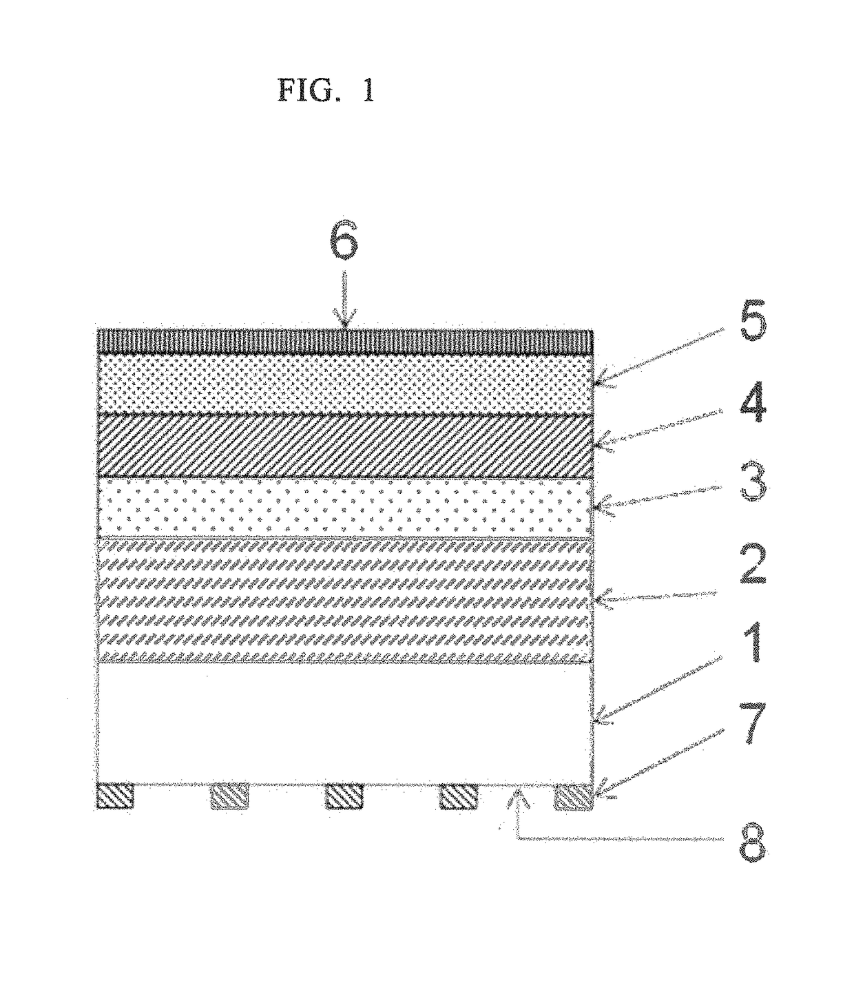
[0091](Preparation of n-Type AlN Single Crystal Substrate 1)

[0092]The n-type AlN single crystal substrate was manufactured by the method described in Applied Physics Express 8 (2015) 061003. Specifically, a C-plane AlN seed substrate having a diameter of 25 mm made by a PVT method (sublimation method) was prepared first. This AlN seed substrate had an off-angle of 0.05 to 0.3° and a dislocation density of not more than 104 cm−2. The AlN seed substrate used had high resistance (specific resistance value: 10 TΩ·cm).

[0093]Next, on the AlN seed substrate, an n-type AlN thick membrane (referred to as a “HVPE process n-type AlN thick membrane” hereinafter) having a thickness of 300 μm was formed by a HVPE process, and thereafter, CMP of the grown plane of the HVPE process n-type AlN thick membrane was carried out. From X-ray rocking curve measurement, it was confirmed that the HPVE process AlN thick membrane after CMP kept a dislocation density of not more than 104 cm−2 similarly to the A...

example 2

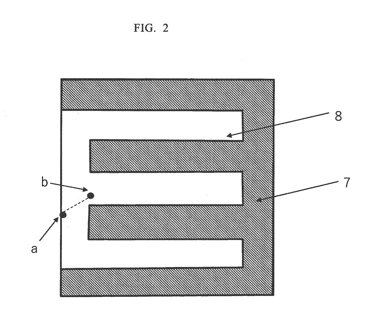
[0108]A vertical light-emitting diode was manufactured in the same manner as in Example 1, except that in the formation of an n-electrode of Example 1, the diameter of the opening was changed to 300 μm (shortest distance: 150 μm). The area of all the openings was 1.77 mm2 (number of openings: 25), and the proportion of the openings to the rear plane area of the chip was 55%.

[0109]The emission wavelength of the manufactured vertical light-emitting diode was 260 nm, and the operating voltage at a driving current of 100 mA was 35 V. The emission intensity distribution (minimum light intensity / maximum light intensity) on the light-emitting plane, as estimated from a near-field image of the light-emitting diode, was 0.87. These results are summarized in Table 1.

example 3

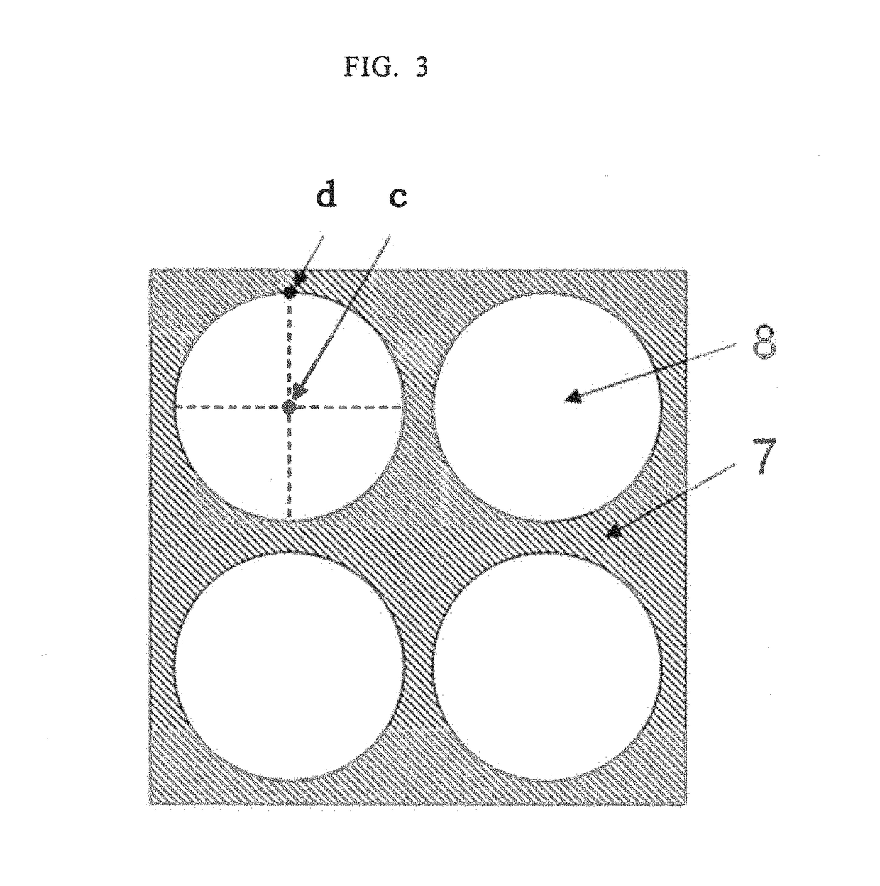
[0110]A vertical light-emitting diode was manufactured in the same manner as in Example 1, except that in the exposure of the rear plane of the n-type AlN single crystal substrate of Example 1, immersion in a 10% KOH aqueous solution was carried out under the conditions of 100° C. and 5 minutes after the CMP of the nitrogen polar plane of the HVPE process n-type AlN substrate. The area of all the openings was 1.77 mm2 (number of openings: 9), and the proportion of the openings to the rear plane area of the chip was 55%. An electron micrograph of the opening is shown in FIG. 8. It was confirmed that on the whole of the n-type AlN single crystal plane, hexagonal pyramids were formed, and the plane angle between the horizontal plane and the hexagonal pyramid was 60 to 63°, and this angle was almost equal to that of the (1-101) plane of AlN.

[0111]The emission wavelength of the manufactured vertical light-emitting diode was 260 nm, and the operating voltage at a driving current of 100 mA...


PUM


Abstract

A vertical ultraviolet light-emitting diode has, on an aluminum polar plane of an n-type AlN single crystal substrate, a layer represented by n-type AlXGa1-XN (wherein X is a rational number satisfying 0.5≤X≤1.0), an active layer, a layer represented by p-type AlYGa1-YN (wherein Y is a rational number satisfying 0.5≤Y≤1.0) and a p-type GaN layer in this order and which is equipped with a p-electrode formed on the p-type GaN layer and an n-electrode partially provided on a plane on the opposite side to the aluminum polar plane of the n-type AlN single crystal substrate, preferably an n-electrode formed by providing at least one opening functioning as a light extraction window, wherein the shortest distance between the n-electrode and an arbitrary point in a portion where the n-electrode is not provided, is not more than 400 μm.

Description

TECHNICAL FIELD[0001]The present invention relates to a vertical ultraviolet light-emitting diode using an n-type AlN (aluminum nitride) single crystal substrate.BACKGROUND ART[0002]A group III nitride semiconductor is a semiconductor material composed of a mixed crystal of indium nitride (InN), gallium nitride (GaN) and aluminum nitride (AlN), and by controlling a composition of a mixed crystal of In, Ga and Al that are group III elements, it becomes possible to manufacture light-emitting elements having high efficiency in a wavelength range of infrared region to ultraviolet region corresponding to their respective band gap energies (0.7 eV (InN), 3.4 eV (GaN) and 6.1 eV (AlN)). On that account, blue light-emitting diodes using the group III nitride semiconductors are now being used for a wide range of applications including illumination, as white light-emitting diodes that are combinations of them and fluorescent materials.[0003]The blue light-emitting diode is formed of an InGaN-...

Claims


Application Information

Patent Timeline
IPC IPC(8): H01L33/38H01L33/06H01L33/32
CPCH01L33/38H01L33/06H01L33/32H01L33/16H01L33/02H01L33/0093H01L21/0262H01L21/0254H01L21/02576H01L21/02579H01L21/02458H01L21/02505H01L21/02433H01L21/02389
Inventor KINOSHITA, TORU
Owner STANLEY ELECTRIC CO LTD
Why Eureka
Try Eureka