Dielectric Film Forming Composition

a technology of dielectric films and compositions, applied in the direction of basic electric elements, electrical apparatus, solid-state devices, etc., can solve the problems of increasing the amount of filler, so as to reduce the effect of reducing the transparency of the film and reducing the amount of cte of the dielectric film

Active Publication Date: 2019-03-14
FUJIFILM ELECTRONICS MATERIALS US
View PDF6 Cites 4 Cited by
  • Summary
  • Abstract
  • Description
  • Claims
  • Application Information

AI Technical Summary

Benefits of technology

[0003]Dielectric material requirements for packaging applications are continuously evolving as new, advanced devices are relying heavily on wafer and panel-level packaging (WLP and PLP) and 3D integration. One of the important requirements of dielectric films for advanced packaging designs is low coefficient of thermal expansion (CTE). In recent years, fillers such as silica particles have been used in the film-forming compositions to lower the CTE of the resulting film. The drawback to this approach is that as the amount of the filler is increased, the transparency of the film decreases and patterning of such a dielectric film by using actinic radiation becomes difficult. In addition, the mechanical properties of such a dielectric film suffer with the increase of the amount of the filler. This disclosure relates to novel compositions that surprisingly reduce the amount of CTE of the dielectric films formed while keeping the films transparent. In addition, the films thus formed retain their mechanical properties such as elongation to break and young modulus.

Problems solved by technology

The drawback to this approach is that as the amount of the filler is increased, the transparency of the film decreases and patterning of such a dielectric film by using actinic radiation becomes difficult.
In addition, the mechanical properties of such a dielectric film suffer with the increase of the amount of the filler.

Method used


Image

  • Dielectric Film Forming Composition
  • Dielectric Film Forming Composition
  • Dielectric Film Forming Composition

Examples


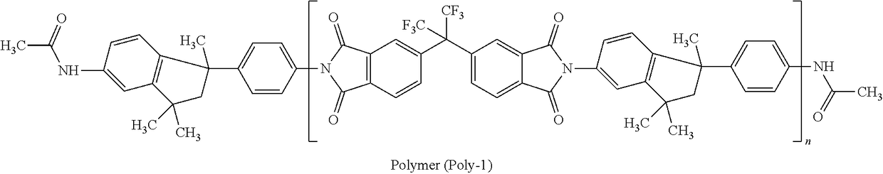
synthesis example 1 (

P-1)

Preparation of 6FDA / DAPI Polyimide

[0110]

[0111]Solid 4,4′-(hexafluoroisopropylidene)bis(phthalic anhydride) (6FDA) (2.370 kg, 5.33 mole) was charged to a solution of 1-(4-aminophenyl)-1,3,3-trimethylindan-5-amine (also known as 4,4′-[1,4-phenylene-bis(1-methylethylidene)]bisaniline (DAPI)) (1.473 kg, 5.51 mole) in NMP (9.86 kg) at 25° C. The reaction temperature was increased to 40° C. and the mixture was allowed to react for 6 hours. Next, acetic anhydride (1.125 kg) and pyridine (0.219 kg) were added and the reaction temperature was increased to 100° C. and allowed to react for 12 hours.

[0112]The reaction mixture above was cooled to room temperature and transferred to a larger vessel equipped with a mechanical stirrer. The reaction solution was diluted with ethyl acetate and washed with water for one hour. After the stirring was stopped, the mixture was allowed to stand undisturbed. Once phase separation had occurred, the aqueous phase was removed. The organic phase was diluted...

formulation example 9

[0121]Formulation Example 9 (FE-9) was prepared by using 13.00 g of polymer (Poly-1), 27.36 g cyclopentanone, 31.20 g cyclohexanone, 1.73 g n-butanol, 0.65 g of methacryloxypropyl trimethoxysilane, 0.39 g of NCI-831, 2.60 g of titanium carboxyethyl acrylate, 7.80 g of surface treated silica, 13 g of tetraethylene glycol diacrylate (SR 268), 1.46 g of trimethylolpropane triacrylate, (SR 351LV), 0.78 g of 0.05% solution of Polyfox 6320 in cyclopentanone, and 0.03 g of p-benzoquinone. After being stirred mechanically for 24 hours, the formulation was used for the following tests.

process example 1

Lithography Process Example 1

[0122]The photosensitive FE-9 was spin coated on a silicon wafer and baked at 70° C. for 180 seconds using a hot plate to form a coating with a thickness of about 15 microns. The photosensitive polyimide film was exposed with a broadband UV exposure tool (Carl Süss MA-56) through a mask having a desired pattern for exposure. After the exposure, the exposed film was heated at 50° C. for 3 minutes.

[0123]After the post exposure bake, unexposed portions were removed by using cyclopentanone as a developer (2×75 seconds of development), followed by rinsing the developed film with PGMEA for 15 seconds to form a pattern. A resolution of 20 microns at a photospeed of 250 mJ / cm2 was achieved. Patterned features in the film exhibited an aspect ratio of 15 / 20 or 0.75.

Laser Ablation Process Example 1

[0124]FE-6 (Table 2) was spin coated on a silicon wafer and baked at 95° C. for 10 minutes using a hot plate to form a coating with a thickness of about 10.50 microns). T...


PUM

PropertyMeasurementUnit
particle sizeaaaaaaaaaa
optical transparencyaaaaaaaaaa

Abstract

This disclosure relates to dielectric film forming composition containing at least one fully imidized polyimide polymer; at least one inorganic filler; at least one metal-containing (meth)acrylate compound; and at least one catalyst. The dielectric film formed by such a composition can have a relatively low coefficient of thermal expansion (CTE) and a relatively high optical transparency.

Description

CROSS-REFERENCE TO RELATED APPLICATIONS[0001]The present application claims priority to U.S. Provisional Application Ser. No. 62 / 581,895, filed on Nov. 6, 2017, and U.S. Provisional Application Ser. No. 62 / 556,723, filed on Sep. 11, 2017. The prior applications are hereby incorporated by reference in their entirety.BACKGROUND OF THE DISCLOSURE[0002]The continued expansion of mobile computing applications requires the packing of ever growing levels of computing power in smaller device footprints. Designers of semiconductor devices are relying on the use of a variety of new chip architectures to meet the new device requirements. These new architectures pose significant challenges not only for the designers of new integrated circuits, but also for the designers of the packaging materials that will be used for these devices.SUMMARY OF THE DISCLOSURE[0003]Dielectric material requirements for packaging applications are continuously evolving as new, advanced devices are relying heavily on ...

Claims


Application Information

Patent Timeline
Patent Type & Authority Applications(United States)
IPC IPC(8): C08G73/10C08J3/24C08K3/36C08J5/18G03F7/038G03F7/16G03F7/20G03F7/38G03F7/32G03F7/40H01L23/373H01L21/02H01L21/268H01L21/311
CPCC08G73/1085C08J3/24C08K3/36C08J5/18G03F7/0387G03F7/162G03F7/168G03F7/2002G03F7/38G03F7/32G03F7/40H01L23/3737H01L21/02118H01L21/02282H01L21/268H01L21/31127C08J2379/08C08K2201/005C09D7/00C08K5/098H01L23/5329H01L21/311G03F7/0047G03F7/202G03F7/0042G03F7/027G03F7/037G03F7/025C08F267/10C09D4/06C09D179/08C08G73/101C08G73/1039C08G73/1067C08F222/102C08F222/105C08F222/1065C08F220/283C08F230/085C08F283/04C08F2/50C08K5/0025C08K3/013C08J5/24C09D7/40H01L21/32134H01L21/76802H01L21/76828H01L21/76865H01L21/76871H01L21/76879C08F222/1006C08G73/1092H01L23/5226H01L23/53228
Inventor MALIK, SANJAYREINERTH, WILLIAM A.DE, BINOD B.
Owner FUJIFILM ELECTRONICS MATERIALS US
Why Eureka
Try Eureka