

Method for manufacturing field effect transistor and method for manufacturing wireless communication device
- Summary
- Abstract
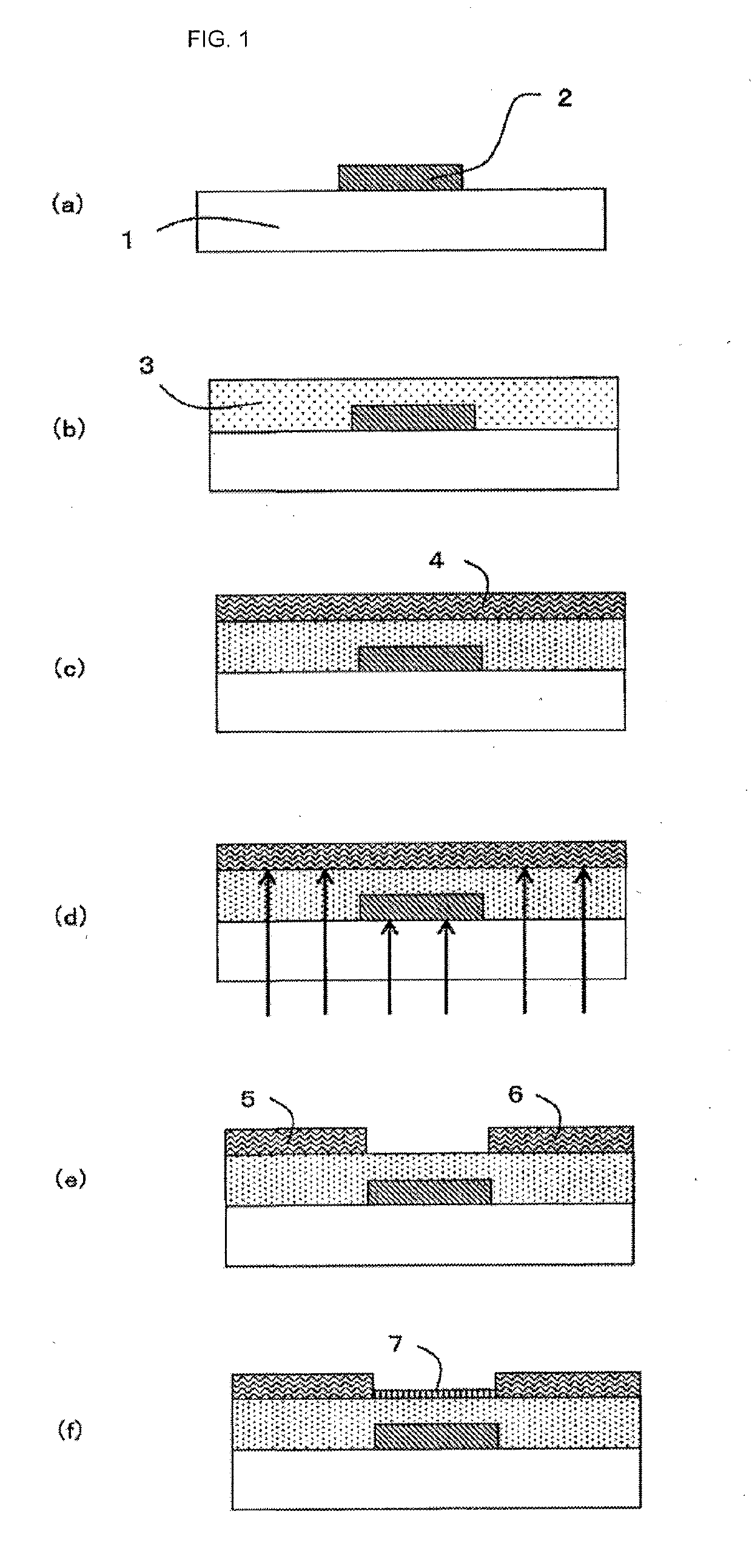
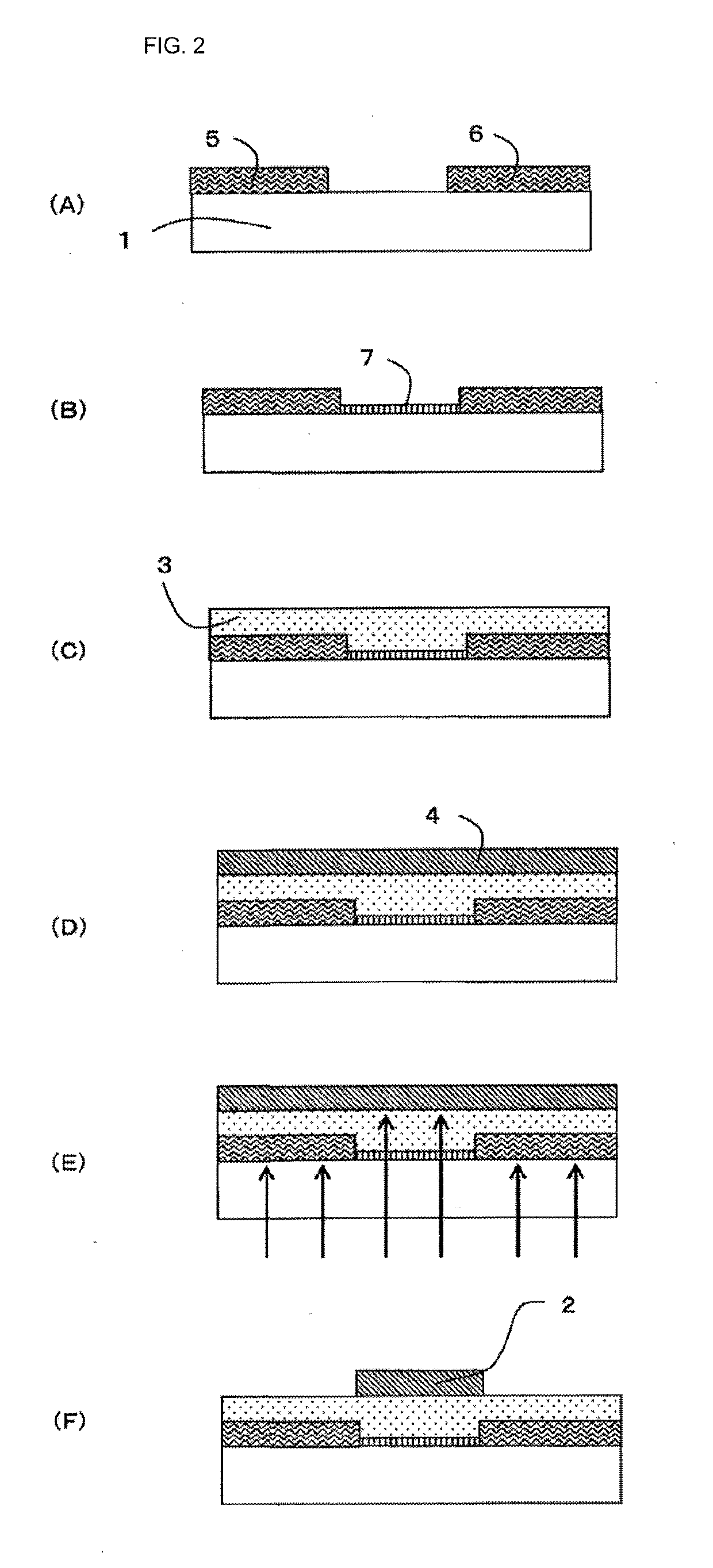
- Description
- Claims
- Application Information
AI Technical Summary
Benefits of technology
Problems solved by technology
Method used
Image

Examples
synthesis example 1
ensitive Organic Component)
[0258]Copolymerization Ratio (mass basis): ethyl acrylate (hereinafter, “EA”) / 2-ethylhexyl methacrylate (hereinafter, “2-EHMA”) / styrene (hereinafter, “St”) / glycidyl methacrylate (hereinafter, “GMA”) / acrylic acid (hereinafter, “AA”)=20 / 40 / 20 / 5 / 15.
[0259]In a reaction container in a nitrogen atmosphere, 150 g of diethylene glycol monoethyl ether acetate (hereinafter, “DMEA”) was put, and the temperature was raised up to 80° C. with the use of an oil bath. Delivered by drops into the container over 1 hour was a mixture composed of 20 g of EA, 40 g of 2-EHMA, 20 g of St, 15 g of AA, 0.8 g of 2,2′-azobisisobutyronitrile, and 10 g of DMEA. After the completion of the dropping, the polymerization reaction was further developed for 6 hours. Thereafter, 1 g of hydroquinone monomethyl ether was added to terminate the polymerization reaction. Subsequently, a mixture composed of 5 g of GMA, 1 g of triethylbenzylammonium chloride, and 10 g of DMEA was delivered by drops...
synthesis example 2
ensitive Organic Component)
[0260]Copolymerization Ratio (mass basis): bifunctional epoxy acrylate monomer (epoxy ester 3002A; manufactured by Kyoeisha Chemical Co., Ltd.) / bifunctional epoxy acrylate monomer (epoxy ester 70 PA; manufactured by Kyoeisha Chemical Co., Ltd.) / GMA / St / AA=20 / 40 / 5 / 20 / 15.
[0261]In a reaction container in a nitrogen atmosphere, 150 g of diethylene glycol monoethyl ether acetate (hereinafter, “DMEA”) was put, and the temperature was raised up to 80° C. with the use of an oil bath. Delivered by drops into the container over 1 hour was a mixture composed of 20 g of epoxy ester 3002A, 40 g of epoxy ester 70PA, 20 g of St, 15 g of AA, 0.8 g of 2,2′-azobisisobutyronitrile, and 10 g of DMEA. After the completion of the dropping, the polymerization reaction was further developed for 6 hours. Thereafter, 1 g of hydroquinone monomethyl ether was added to terminate the polymerization reaction. Subsequently, a mixture composed of 5 g of GMA, 1 g of triethylbenzylammonium c...
synthesis example 3
ensitive Organic Component)
[0262]Urethane-modified Compound of Compound P2 In a reaction container in a nitrogen atmosphere, 100 g of diethylene glycol monoethyl ether acetate (hereinafter, “DMEA”) was put, and the temperature was raised up to 80° C. with the use of an oil bath. Delivered by drops into the container over 1 hour was a mixture composed of 10 g of the photosensitive component P2, 3.5 g of n-hexyl isocyanate, and 10 g of DMEA. After the completion of the dropping, the reaction was further developed for 3 hours. The obtained reaction solution was purified with methanol to remove unreacted impurities, and further dried in vacuum for 24 hours to obtain a compound P3 having an urethane bond.
PUM
 Abstract
Description
Claims
Application Information