Method for depositing silicon-free carbon-containing film as gap-fill layer by pulse plasma-assisted deposition

Active Publication Date: 2020-01-09
ASM IP HLDG BV
View PDF24 Cites 177 Cited by
  • Summary
  • Abstract
  • Description
  • Claims
  • Application Information

AI Technical Summary

Benefits of technology

[0036]This disclosure provides a structure formed by filling a patterned recess of a substrate by the steps of: (a) providing the substrate in a reaction space; (b) providing a precursor to the reaction space, thereby filling the recess with a gas phase precursor; (c) providing a plasma to the reactio

Problems solved by technology

However, with miniaturization of wiring pitch of large scale integration (LSI) devices, void-free filling of high aspect ratio spaces (e.g., AR≥3) becomes increasingly difficult due to limitations of existing deposition processes.
However, it is difficult to find suitable combinations of an inhibitor and an activator, and to find suitable process conditions for deposition.
In many cases, it is not practical.
However, when the trench is deeper, in order to bombard a bottom area of the trench with ions, the mean free path of ions has to be made longer to reach the bottom area by, e.g., significantly reducing pressure to a hard vacuum, which is often costly and unpractical.
Also, when the layer is expanded and closes the trench, the layers facing eac

Method used


Image

  • Method for depositing silicon-free carbon-containing film as gap-fill layer by pulse plasma-assisted deposition
  • Method for depositing silicon-free carbon-containing film as gap-fill layer by pulse plasma-assisted deposition
  • Method for depositing silicon-free carbon-containing film as gap-fill layer by pulse plasma-assisted deposition

Examples


Example

Example 1

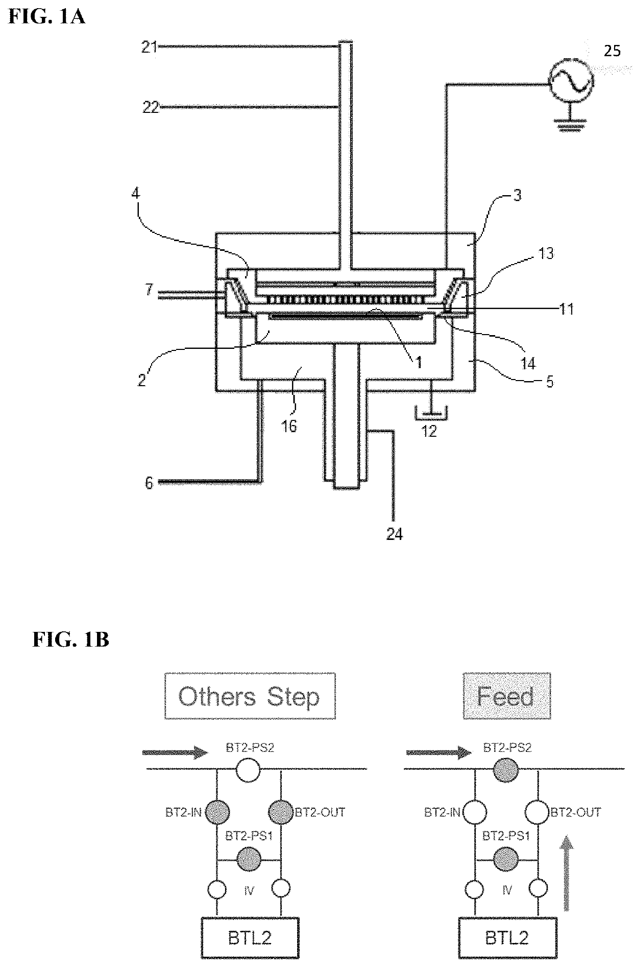
[0117]A Si-free C-containing film was deposited on a Si substrate (having a diameter of 300 mm and a thickness of 0.7 mm) having narrow / deep trenches with an opening of approximately 20 nm, which had a depth of approximately 200 nm (an aspect ratio was approximately 10), and narrow / shallow trenches with an opening of approximately 20 to 35 nm, which had a depth of approximately 90 nm, by PEALD-like process in order to determine filling capability of the film, under the conditions shown in Table 5 below using the apparatus illustrated in FIG. 1A and a gas supply system (FPS) illustrated in FIG. 1B. A carrier gas (its flow rate was 0.1 slpm) was used to feed the precursor to the reaction chamber. However, the carrier gas is not required because of the high vapor pressure of the precursor. In this example, small mass flow of the carrier was used just as a precaution against precursor condensation in the line. If the line is sufficiently heated, no carrier gas need be used. Fur...

Example

Comparative Example 1

[0119]A Si-free C-containing film was deposited on a Si substrate in a manner substantially similar to that in Example 1 except that the total of He flow was 1.5 slm, the gap (between capacitively coupled electrodes) was 16 mm, the total pressure was 800 Pa, the duration of RF application pulse was 1.2 seconds, and the number of cycles was 93. Further, the substrate had narrow trenches with an opening of approximately 30 nm, which had a depth of approximately 90 nm (an aspect ratio was approximately 3), intermediate trenches with an opening of approximately 70 nm, which had a depth of approximately 90 nm (an aspect ratio was approximately 1.3), and wide trenches with an opening of approximately 100 nm, which had a depth of approximately 90 nm (an aspect ratio was approximately 0.9).

[0120]FIG. 11 shows STEM photographs of cross-sectional views of wide trenches subjected to gap-fill cycles in (a), wide and narrow trenches subjected to gap-fill cycles in (b), and n...

Example

Example 2

[0121]A Si-free C-containing film was deposited on a Si substrate in a manner substantially similar to that in Example 1, and the properties of the film were evaluated. The results are shown in Table 6 below.

TABLE 6(numbers are approximate)Propertiesa-C gapfillDR (nm / min)15R.I. (@633 nm)1.57Contact angle (degree)66Stress (MPa)0Thermal@050 C., 30 min in N20Stability@100 C., 30 min in N210-20(Shrinkage %)@200 C., 30 min in N210-20@300 C., 30 min in N235-40AshableO2 / ArYesN2 / H2YesFillingAR3, CD30GoodcapabilityAR10, CD10GoodAR10, CD20GoodDensityRBS0.75(g / cm3)Composition(+ / −3%)C (%)49.0H (%)49.5O (%)1.5

[0122]In the above, RBS stands for Rutherford backscattering spectrometry, SIMS stands for Secondary-ion mass spectrometry, AR stands for aspect ratio, DR stands for deposition rate, CD stands for critical dimensions (nm), and RI stands for reflective index. As shown in Table 6, the film was constituted substantially by carbon and hydrogen, which was considered to be amorphous carb...


PUM

PropertyMeasurementUnit
Temperatureaaaaaaaaaa
Fractionaaaaaaaaaa
Fractionaaaaaaaaaa

Abstract

A film having filling capability is deposited by forming a viscous polymer in a gas phase by striking an Ar, He, or N2 plasma in a chamber filled with a volatile hydrocarbon precursor that can be polymerized within certain parameter ranges which define mainly partial pressure of precursor during a plasma strike, and wafer temperature.

Description

CROSS-REFERENCE TO RELATED APPLICATIONS[0001]This application is a continuation-in-part of U.S. patent application Ser. No. 16 / 026,711, filed Jul. 3, 2018, the disclosure of which is herein incorporated by reference in its entirety.BACKGROUNDField of the Invention[0002]The present invention generally relates to a method for depositing a silicon-free carbon-containing film as a gap-fill layer in trenches by pulse plasma-assisted deposition.Description of the Related Art[0003]In processes of fabricating integrated circuits such as those for shallow trench isolation, inter-metal dielectric layers, passivation layers, etc., it is often necessary to fill trenches (any recess typically having an aspect ratio of one or higher) with insulating material. However, with miniaturization of wiring pitch of large scale integration (LSI) devices, void-free filling of high aspect ratio spaces (e.g., AR≥3) becomes increasingly difficult due to limitations of existing deposition processes.[0004]FIG. ...

Claims


Application Information

Patent Timeline
IPC IPC(8): H01L21/02H01L21/762H01L21/768
CPCH01L21/76837H01L21/02205H01L21/0228H01L21/76229H01L21/02118H01L21/02274C23C16/26C23C16/45542C23C16/50H01L21/76224H01L21/02115
Inventor BLANQUART, TIMOTHEE JULIEN VINCENTUTSUNO, MITSUYASUSA, YOSHIOFUKAZAWA, ATSUKINAKANISHI, TOSHIO
Owner ASM IP HLDG BV
Why Eureka
Try Eureka