Amorphous oxide semiconductor film, oxide sintered body, and thin film transistor

a semiconductor film and amorphous oxide technology, applied in the direction of transistors, vacuum evaporation coatings, coatings, etc., can solve the problem that the patent literature 1 does not disclose any oxide semiconductors, and achieve the effect of small change in properties and high carrier mobility

Active Publication Date: 2020-02-13
IDEMITSU KOSAN CO LTD
View PDF0 Cites 0 Cited by
  • Summary
  • Abstract
  • Description
  • Claims
  • Application Information

AI Technical Summary

Benefits of technology

[0019]Meanwhile, there exists strong demand for higher-quality TFT, and for a material e...

Problems solved by technology

However, Patent Literature 1 doe...

Method used


Image

  • Amorphous oxide semiconductor film, oxide sintered body, and thin film transistor
  • Amorphous oxide semiconductor film, oxide sintered body, and thin film transistor
  • Amorphous oxide semiconductor film, oxide sintered body, and thin film transistor

Examples


examples

[0259]An aspect(s) of the invention will be described below with reference to Examples and Comparatives. It should however be noted that the scope of the invention is not limited to Examples.

Preparation of Sintered Oxide

examples 1 to 3

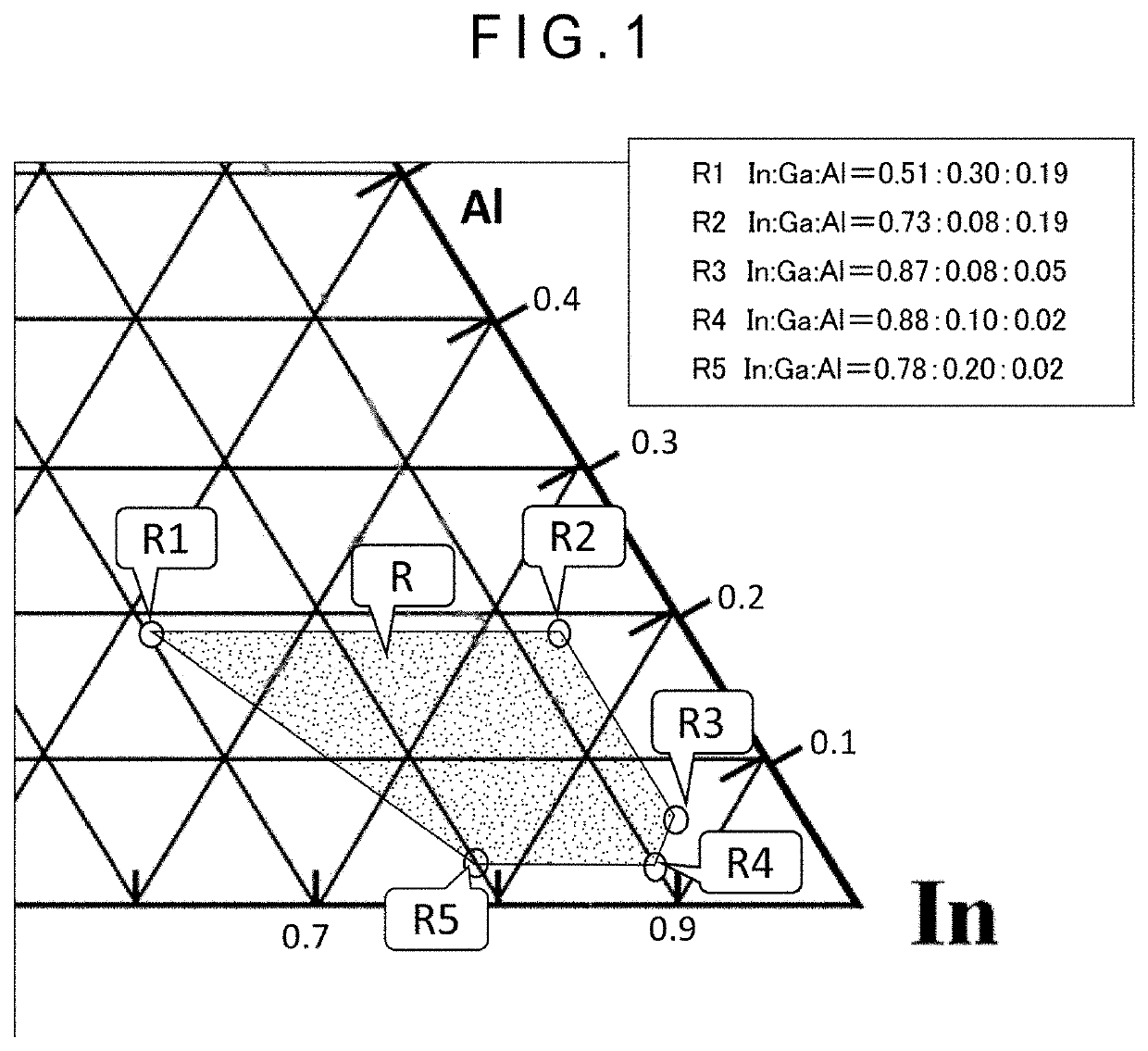
[0260]Powders of gallium oxide, aluminum oxide, and indium oxide were weighed in an atomic ratio as shown in Table 1, which were put in a polyethylene pot and mixed / pulverized using a dry ball mill for 72 hours to prepare a mixture powder.

[0261]The mixture powder was put in a die and pressed at a pressure of 500 kg / cm2 to prepare a molding body. The molding body was compacted through CIP at a pressure of 2000 kg / cm2. Next, the molding body was placed in an atmospheric-pressure sintering furnace and was kept at 350 degrees C. for 3 hours. Subsequently, the temperature inside the furnace was raised at a temperature increase rate of 100 degrees C. / hr., was kept at 1450 degrees C. for 32 hours, and was left and cooled to obtain a sintered oxide.

[0262]The following items of the obtained sintered oxide were evaluated. The results are shown in Table 1.

Property Evaluation of Sintered Oxide

(1) XRD Measurement

[0263]XRD (X-Ray Diffraction) of the obtained sintered oxide was measured using an X...

example a

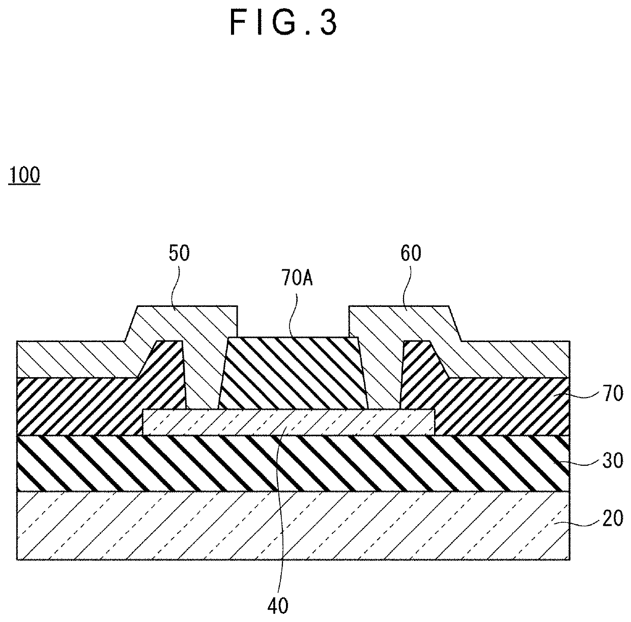
[0281]A thin-film transistor was prepared according to a process below.

(1) Film-Formation Step

[0282]A sintered oxide prepared in Example 1 was ground and polished to prepare a sputtering target of 4-inch diameter×5 mm-thick. At this time, the sputtering target was smoothly prepared without causing cracks or the like. A 50-nm thin film (oxide semiconductor layer) was formed on a silicon wafer 20 (gate electrode) coated with a thermally oxidized film (gate insulating film) through sputtering via a metal mask using the prepared sputtering target under the film-formation conditions shown in Table 2. At this time, sputtering gas in a form of mixture gas of high-purity argon and 1% high-purity oxygen was used for sputtering.

[0283]Further, a sample provided solely with a 50-nm-thick oxide semiconductor layer on a glass substrate was simultaneously prepared under the same conditions. The glass substrate was made of ABC-G manufactured by Nippon Electric Glass Co., Ltd.

(2) Formation of Source...


PUM

PropertyMeasurementUnit
Angleaaaaaaaaaa
Angleaaaaaaaaaa
Angleaaaaaaaaaa

Abstract

A sintered oxide includes an In2O3 crystal, and a crystal A whose diffraction peak is in an incidence angle (2θ) range defined by (A) to (F) below as measured by X-ray (Cu—K α ray) diffraction measurement: 31.0 to 34.0 degrees . . . (A); 36.0 to 39.0 degrees . . . (B); 50.0 to 54.0 degrees . . . (C); 53.0 to 57.0 degrees . . . (D); 9.0 to 11.0 degrees . . . (E); and 19.0 to 21.0 degrees . . . (F).

Description

TECHNICAL FIELD[0001]The present invention relates to an amorphous oxide semiconductor film, a sintered oxide, and a thin-film transistor.BACKGROUND ART[0002]Amorphous oxide semiconductor usable for a thin-film transistor has higher carrier mobility than general-purpose amorphous silicon (a-Si) and a large optical band gap, and can form a film at a low temperature. Accordingly, the use of the amorphous oxide semiconductor is expected in the field of next-generation display devices requiring high-resolution and high-speed large-size image display, and a resin substrate with low heat resistance. The oxide semiconductor (film) is suitably formed through a sputtering process, in which a sputtering target is sputtered. This is because a thin film formed through the sputtering process is more excellent in terms of in-plane uniformity (e.g. composition uniformity in a film plane direction (i.e. within a film plane) and even film thickness) than a thin film formed through ion-plating proces...

Claims


Application Information

Patent Timeline
IPC IPC(8): H01L29/786C23C14/08H01L21/203H01L27/12C23C14/34
CPCH01L21/203C23C14/086C23C14/34H01L27/1222H01L29/78693C04B35/01H01L21/02565H01L21/02631H01L27/1225H01L29/66969C23C14/3414C23C14/5806C23C14/024C04B35/64C04B2235/77C04B2235/80C04B2235/761C04B2235/3217C04B2235/3286C04B2235/604C04B2235/6562C04B2235/658C04B2235/6567C23C14/08C04B35/10C23C14/3407H01L29/66439H01L21/20
Inventor INOUE, KAZUYOSHISHIBATA, MASATOSHI
Owner IDEMITSU KOSAN CO LTD
Why Eureka
Try Eureka