Organometallic metal chalcogenide clusters and application to lithography

a technology of organic chalcogenide and clusters, applied in the field of organic chalcogenide clusters and application to lithography, can solve the problems of affecting the dissolution rate of selected solvents, and achieve the effect of less soluble in organic solvents

Pending Publication Date: 2021-01-28
INPRIA CORP
View PDF2 Cites 4 Cited by
  • Summary
  • Abstract
  • Description
  • Claims
  • Application Information

AI Technical Summary

Benefits of technology

[0007]In a second aspect, the invention pertains to a coated substrate comprising a radiation sensitive film of (RSn)4X6 having an average thickness of no more than 1 micron and a thickness variation no more than 25% from the average at any point across the film. The coating comprises a metal-sulfide (selenide) network with metal cations having organic ligands with metal-carbon bonds or a metal-sulfide-oxide-hydroxide network with metal cations attached to organic ligands via metal-carbon bonds. In some embodiments, this aspect can be described as a structure with a radiation sensitive patterning layer comprising a substrate and a radiation sensitive layer comprising organotin clusters represented by the formula (RSn)4X6 wherein R is an organic ligand having 1 to 15 carbon atoms bound to Sn with a metal-carbon bond, and X is S or Se wherein the radiation sensitive layer has an average thickness from about 2 nm to about a micron.
[0008]In a third aspect, the invention pertains to a method for patterning a radiation-sensitive coating of (RSn)4X6, the method comprising the steps of irradiating the coated substrate along a selected pattern to form an irradiated structure with regions of irradiated coating and regions of un-irradiated coating and selectively developing the irradiated coating to remove a substantial portion of the un-irradiated regions. The coated substrate generally comprises a coating comprising metal-sulfide clusters or a metal-sulfide network with metal cations having organic ligands with metal-carbon bonds or a metal-sulfide-oxide-hydroxide network with metal cations attached to organic ligands via metal-carbon bonds. More specifically, this aspect can be described as a method of patterning a coating, in which the method comprises developing a pattern from a virtual image formed by subjecting a radiation sensitive layer to a radiation pattern to form an irradiated layer. The developing of the pattern can comprise contacting the irradiated layer with an organic solvent to remove substantially an un-irradiated portion of the irradiated layer, in which the radiation sensitive layer is formed with organotin clusters, and wherein irradiation of the radiation sensitive layer results in a material substantially less soluble in organic solvents.

Problems solved by technology

Radiation can alter the chemical structure and composition of a photoresist and thereby affect its dissolution rate in a selected solvent.

Method used


Image

  • Organometallic metal chalcogenide clusters and application to lithography
  • Organometallic metal chalcogenide clusters and application to lithography
  • Organometallic metal chalcogenide clusters and application to lithography

Examples


example 4

ed Wafers

[0082]This example describes the preparation of film-coated wafers and demonstrates that thin and smooth films can be deposited for both the n-butyltin and the n-butenyltin cluster compositions.

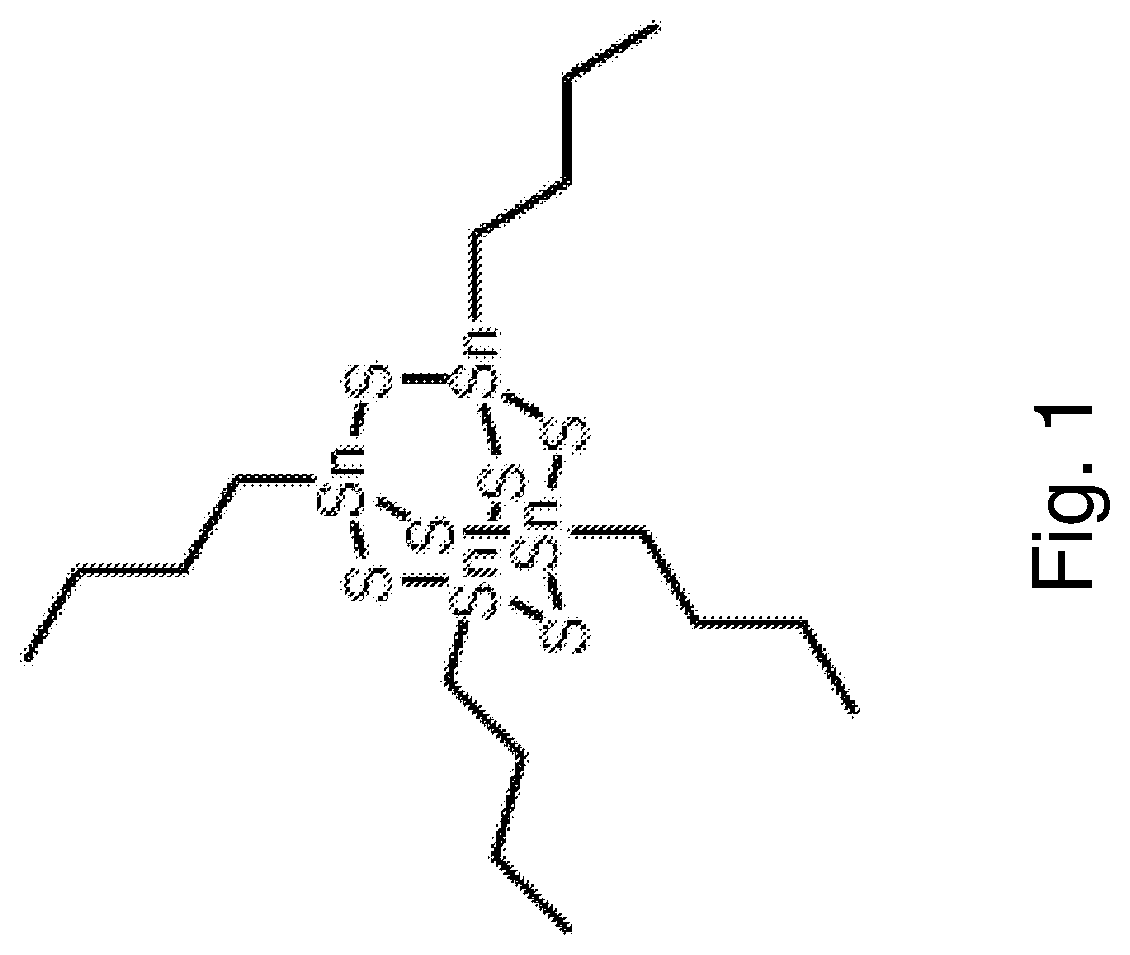
[0083]Silicon wafers (10.2-cm diameter) with a native-oxide surface served as substrates for thin-film deposition. Unless otherwise indicated, films were deposited on untreated wafers by spin coating toluene-based precursor solutions, prepared as described in Example 3, onto untreated wafers at 1500 rpm for 30 seconds. In some cases, wafers were pre-treated by wetting with casting solvent if useful to obtain a good coating. Specifically, a precursor solution of (C4H9Sn)4S6 (R1) in toluene having a tin concentration of 75 mM was spin coated onto a wafer at 1500 rpm for 30 seconds to produce a film sample (F1) with a film of thickness 176 nm. A second precursor solution of (C4H7Sn)4S6 (R2) in toluene having a tin concentration of 75 mM was spin coated onto a wafer at 1500 rpm for 30 se...

example 5

Tone Imaging with UV Exposure

[0086]This example demonstrates that UV radiation can induce negative tone dissolution contrast in films prepared from n-butyltin and n-butenyltin cluster compositions.

[0087]Film samples F1 and F2, prepared as described in Example 4, were placed in a box lined with aluminum foil within an argon-filled glovebox. Sections of film samples F1 and F2 were exposed to laboratory UV light to provide radiation at a wavelength of around 354 nm for some minutes for all of the samples uniformly to provide an appropriate dose, resulting in film samples F1 and F2 each having regions of exposed and unexposed film. The film samples were then developed by submerged for 30 seconds in a mixture of anisole and THF. For each anisole:THF mixture, the film thickness was measured for the exposed and unexposed sections of each film sample using a J. A. Woollam M-2000 spectroscopic ellipsometer. The normalized film thickness was calculated as the thickness of the developed sectio...

example 6

y Contrast Via EUV Exposure

[0091]This example demonstrates solubility contrast in films from Example 3 after exposure to EUV radiation.

[0092]Films were deposited as described in Example 4 onto 10.2-cm diameter silicon wafers with a native oxide surface. Precursor solutions of (C4H9Sn)4S6 and (C4H7Sn)4S6 were prepared with a concentration suitable to deposit films of R1 and R2, respectively, each film with a thickness of approximately 20 nm. For the contrast curves shown in FIG. 16 and FIG. 17, film thickness ranged between 20.6 nm and 22.9 nm.

[0093]Films were exposed on the EUV Direct Contrast Tool at Lawrence Berkeley National Laboratory. Prior to exposure, the films were baked at 100° C. for 2 minutes. A linear array of 50 circular exposure regions ˜500 μm in diameter were projected onto the wafer with increasing EUV exposure doses. After exposure, the films were developed with 2-heptanone, THF, a 20% (v / v) mixture of anisole in THF, or a 40% (v / v) mixture of anisole in THF. Films...


PUM

PropertyMeasurementUnit
thicknessaaaaaaaaaa
thicknessaaaaaaaaaa
wavelengthaaaaaaaaaa

Abstract

Patterning with UV and EUV light is described with organo tin sulfide (and selenide) clusters. The clusters are solids at room temperature and are soluble in organic solvents that are not too polar. Irradiation can either fragment a carbon metal bond or crosslink unsaturated organic moieties to stabilize the irradiated material. The irradiated material then resists dissolving in organic solvents so that the un-irradiated material can be contacted with an organic solvent to develop the latent image formed with the radiation. Radiation patternable layers can be formed through coating a solution or through vapor deposition. Corresponding precursor solutions, structures and methods are described.

Description

CROSS REFERENCE TO RELATED APPLICATIONS[0001]This application claims priority to copending U.S. provisional patent application 62 / 876,842, filed Jul. 22, 2019 to Cardineau et al., entitled “Organometallic Metal Chalcogenide Clusters and Application to Lithography,” incorporated herein by reference.FIELD OF THE INVENTION[0002]The invention relates to organometallic photoresist compositions and methods to form photoresist coatings and patterns using the compositions.BACKGROUND OF THE INVENTION[0003]In semiconductor manufacturing, materials are patterned to fabricate devices and circuits. These patterned structures are generally formed through an iterative photolithographic process of thin film deposition, radiation exposure, and etch steps to produce a large number of devices in a small area. Advances in the art can involve an increase in device density, which can be desirable to enhance performance.[0004]Thin-film coatings of organic and organometallic compositions can be used as rad...

Claims


Application Information

Patent Timeline
Patent Type & Authority Applications(United States)
IPC IPC(8): G03F7/004C07F7/22G03F7/16G03F7/32G03F7/20
CPCG03F7/0042C07F7/226G03F7/162G03F7/2004G03F7/0048G03F7/32G03F7/167G03F7/0045G03F7/325G03F7/0043
Inventor CARDINEAU, BRIAN J.EARLEY, WILLIAMWAMBACH, TRUMAN
Owner INPRIA CORP
Why Eureka
Try Eureka