CMOS Compatible Material Platform for Photonic Integrated Circuits

a photonic integrated circuit and material platform technology, applied in the direction of instruments, optical elements, optical waveguide light guides, etc., can solve the problems of low energy efficiency, difficult to generate needed light sources, and low optical loss, and achieve the effect of low optical loss

Active Publication Date: 2021-03-18
LI DONG +1
View PDF0 Cites 0 Cited by
  • Summary
  • Abstract
  • Description
  • Claims
  • Application Information

AI Technical Summary

Benefits of technology

[0013]Evanescence coupling feature, with mode matching structures in both layers, is used to optically couple the device in the moderate refractive index (contrast) material with the those within bonded Si layer with minimal optical loss.
[0016]With such as comprehensive heterogeneously integrated photonic material platform system, multiple materials with their own merits can be used to target for the best performance and lowest optical loss, as well as special functionality, which could be unique for a particular material. By doing so, we could build very complicated photo system to meet the challenges for photonic artificial neural network, quantum computer, large scale optical switch, larger than lithography step field passive and active photonic interposer for various applications.

Problems solved by technology

All these material platforms have developed many optical building blocks (or devices) on its own and each platform has it own advantages and disadvantage.
Unfortunately, none of platforms have a comprehensive set of needed building blocks with the best performance, energy efficiency, and cost to offer to design engineers a sweet solution to meet the needs for circuit designs such as full optical neural network.
Firstly, Si is a indirect bandgap materials, therefore it is not easy to generate needed light source in Silicon; Secondly, due to the large refractive index contrast between Si (˜3.5) and SiO2 (˜1.5), the optical loss and phase of the lightwave is very sensitive to any fabrication error during wafer processes.
As such, it is very hard to develop complicated passive (de)multiplexers such as arrayed waveguide grating (AWG), or planar concave grating (PCG); Thirdly, due to Si waveguide for single optical mode has width below one microns meter, to extend the optical circuit larger than the lithography step field size the stitch error between the step fields can generate some overlay errors, which generates unintended bounced wave to disturb the coherence and optical phase, which is extremely important for coherent optic chips like those used in photonic artificial neural networks and quantum computing; Fourthly, silicon have low absorption losses in the wavelength range from 1.1 μm (band edge of silicon) to about 3.7 μm (onset of mid-IR absorption of silica).
For applications requiring shorter wavelengths (e.g. data communication at 850 nm, sensors operating in the therapeutic window etc.) silicon waveguide is not an option; Fifthly, silicon has two photo absorption (TPA) related to Kerr effects, therefore, it has power limitation; Sixthly, the large refractive index contrast also make the mode expansion is no that easy, alignment and coupling efficiency is not as good as the medium refractive contrast system such as silicon nitride (core) / silicon oxide (cladding) system.
This integration approach has a few major disadvantages: 1) due to the SOI circuit particularly the implantation already in place as well as Ge epi-growth over Si for photodiode (Ge PD), the deposition temperature for addon new materials such as SiN has some tight limit to avoid implanted ions' diffusion or existing Ge PDs damage.
Therefore, stoichiometric Si3N4 can not be obtained; 2) potential plasma radiation damage of existing during addon material deposition process; 3) the addon material changes the process and integration scheme of electric connection processes for Ge photodiode (for PECVD SiN) or existing active devices in the SOI layer.
All these bring some hard technology and process limitations, for example, the SiN integrated in such a way can not be used to build passive (de)multiplexers with performance matching those build in stoichiometric Si3N4 deposited by Low Pressure Chemical Vapour Deposition (LPCVD) at high temperature (>700 C) followed by high-than-1000 C annealing for removing N—H and Si—H bonds, which has high optical absorption around 1520 nm.
As such, SOI-first-approach can not offer a good material properties for diamond based optical circuit and its particular functionality.

Method used


Image

  • CMOS Compatible Material Platform for Photonic Integrated Circuits
  • CMOS Compatible Material Platform for Photonic Integrated Circuits
  • CMOS Compatible Material Platform for Photonic Integrated Circuits

Examples


Embodiment Construction

lass="d_n">[0023]The following numerous specific detail descriptions are set forth to provide a thorough understanding of various embodiments of the present disclosure. It will be apparent to one skilled in the art, however, these specific details need not be employed to practice various embodiments of the present disclosure. In other instances, well known components or methods have not been described.

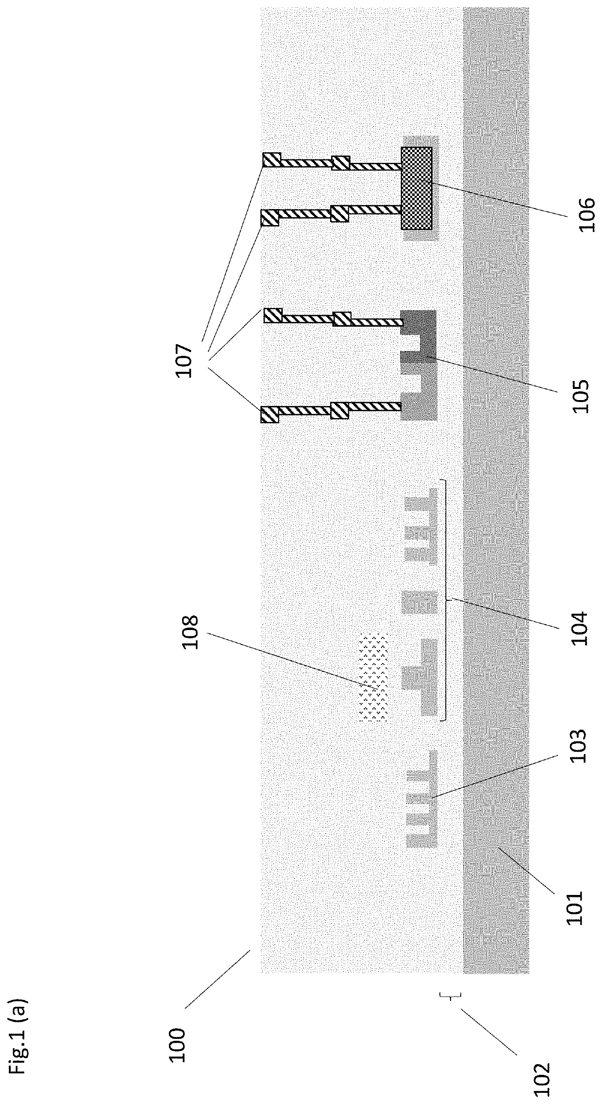
[0024]FIG. 1(a) shows an embodiment of the existing silicon on insulator (SOI) platform 100 with SiN integrated on top of the patterned SOI layer. In details, the incoming SOI wafer has Si substrate 101 with buried oxide (BOX) layer 102. In the SOI layer, various photonic building blocks (devices), such as grating 103, different waveguide structures for the light routing, electrical to optical modulator 105, and Ge photodiode (Ge PD) 106. The active devices such as modulator 105 and Ge PD 106 is connected to vertical electrical connection paths 107. On top of the SOI layer, there is a ...


PUM

PropertyMeasurementUnit
wavelengthaaaaaaaaaa
wavelengthsaaaaaaaaaa
refractive indexaaaaaaaaaa

Abstract

A CMOS compatible heterogeneously integrated material platform for photonic integrated circuitry is invented. The material platform has SiO2 as cladding material, at least a bottom layer made of moderate refractive index (contrast) material(s), a bonded single crystal Si layer transfer from either a SOI wafer or a ion implanted single crystal Si wafer ready for ion cut split on top of the bottom layer, and some devices enabling light coupling between the devices made within these two layers. The invention provides a great material platform to offer a full set of photonic building blocks for all sorts of different applications such as photonic circuitry for optical neural network, quantum computing, telecommunication, data communication, optical switching, optical sensing, passive and / or active Si optical interposer with its size even bigger than lithography step field.

Description

FIELD OF INVENTION[0001]The invention is related to material platform and process integration solutions for large scale CMOS compatible photonic integrated circuits. Particularly, using wafer-to-wafer and optical-material-stack die-to-wafer bonding enable vertically heterogeneous integration of different optical material on a single wafer substrate with medium refractive index contrast optical material close to substrate first before single crystal Si layer bonded next, then other material either over Si or over the bottom layer. There is optical coupling paths between the devices made in different material layers.BACKGROUND ART[0002]Photonic integrated circuits starting from communication applications has been attracted more and more attention and expand its applications in the areas of photonic artificial neural network chips for AI algorithm processing / calculation; photonic chips for quantum computation; photonic chips for data processing for RF / microwave; large scale optical swi...

Claims


Application Information

Patent Timeline
Patent Type & Authority Applications(United States)
IPC IPC(8): G02B6/12H01L25/04G02B1/00G02B6/42
CPCG02B6/12019H01L25/041G02B6/4257G02B1/005G02B6/12014G02B6/12004G02B6/1228
Inventor LI, DONGYI, GE
Owner LI DONG
Why Eureka
Try Eureka