Compound semiconductor epitaxial wafer

a semiconductor and epitaxial wafer technology, applied in semiconductor/solid-state device manufacturing, semiconductor devices, electrical appliances, etc., can solve the problems of increasing stress, reducing the internal quantum efficiency of light emitting diodes, and increasing the stress, so as to prevent misfit dislocation, effectively eliminate stress, and reduce the ascending rate of alloy compositions

Inactive Publication Date: 2000-05-02
SHIN-ETSU HANDOTAI CO LTD
View PDF4 Cites 11 Cited by
  • Summary
  • Abstract
  • Description
  • Claims
  • Application Information

AI Technical Summary

Benefits of technology

For the purpose of solving the above problems, the inventors of the present application have studied hard how to prevent a misfit dislocation from propagating to a composition constant layer and to effectively eliminate a stress caused by lattice mismatching; and have found from their studies that it is good not to lower the ascending rate of an alloy composition to provide a moderate composition change as known as common knowledge in the prior art, but, to the contrary to the prior art, to provide an abrupt change of the alloy composition and immediately thereafter to somewhat descend the alloy composition backward moderately.
That is, the inventors have noted that the alloy composition is abruptly ascended at appropriate positions in a layer thickness direction in order to locally relax a stress accumulated distributedly in the layer thickness direction due to the lattice mismatching, and immediately thereafter the alloy composition is partially descended moderately thereby to prevent reduction of a crystal quality, and that part of the layer whose alloy composition was abruptly ascended is used as a reflective layer to return light upwardly passed therethrough in the substrate direction to thereby improve a luminance.
With the compound semiconductor epitaxial wafer in accordance with this invention, within the alloy composition gradient layer, at least one combination of the alloy composition abruptly ascended with a large rate and the alloy composition relatively moderately descended following the above is formed as distributed in the layer thickness direction. Since the combination of the abrupt increase and slow decrease of the alloy composition enables local relaxation of stresses generated and distributed in the layer thickness direction by lattice constant mismatching, a high quality of epitaxial wafer can be realized. Simultaneously the abrupt ascent of the alloy composition enables formation of a thinner alloy composition gradient layer. As a result, absorption amount of emitted light depending on the layer thickness can be suppressed. Further, since the layer having the abruptly ascended alloy composition functions as a reflective layer, emitted light passed through the substrate can be reflected to its epitaxial growth direction to improve luminance with its external quantum efficiency increased. Further, by the formation of the thinner alloy composition gradient layer, a productivity can be improved.
The composition adjustment zone A13 provided after formation (at the position d16) of the crystal stabilizing zone S13 makes the alloy composition x coincide with a predetermined alloy composition a of the composition constant layer 5 at the position d17. Within the alloy composition gradient layer, when the alloy composition x of the arsenic As is ascended in a range not exceeding the alloy composition a as its target value, stress relaxation can be efficiently attained.
The gift of the embodiment of this invention is that the combination of the abrupt composition ascending zone and relatively moderate crystal stabilizing zone is formed repetitively once or more times, that is, the alloy composition is efficiently ascended while the relaxation of the stress caused by the lattice mismatching distributed in the layer thickness direction is effectively carried out locally. As a result, since the alloy composition gradient layer is made thinner and a reflective layer is provided, the luminance can be improved.

Problems solved by technology

When this dislocation propagates a composition constant layer, however, this results in that the internal quantum efficiency of the light emitting diode drops.
However, this results in that a stress caused by the lattice mismatching gradually accumulates in the entire epitaxial layer and amounts to a larger stress.
This leads to generation of a misfit dislocation in the composition constant layer, with the result of reduction in lifetime and reduction in luminance.

Method used


Image

  • Compound semiconductor epitaxial wafer
  • Compound semiconductor epitaxial wafer
  • Compound semiconductor epitaxial wafer

Examples


Embodiment Construction

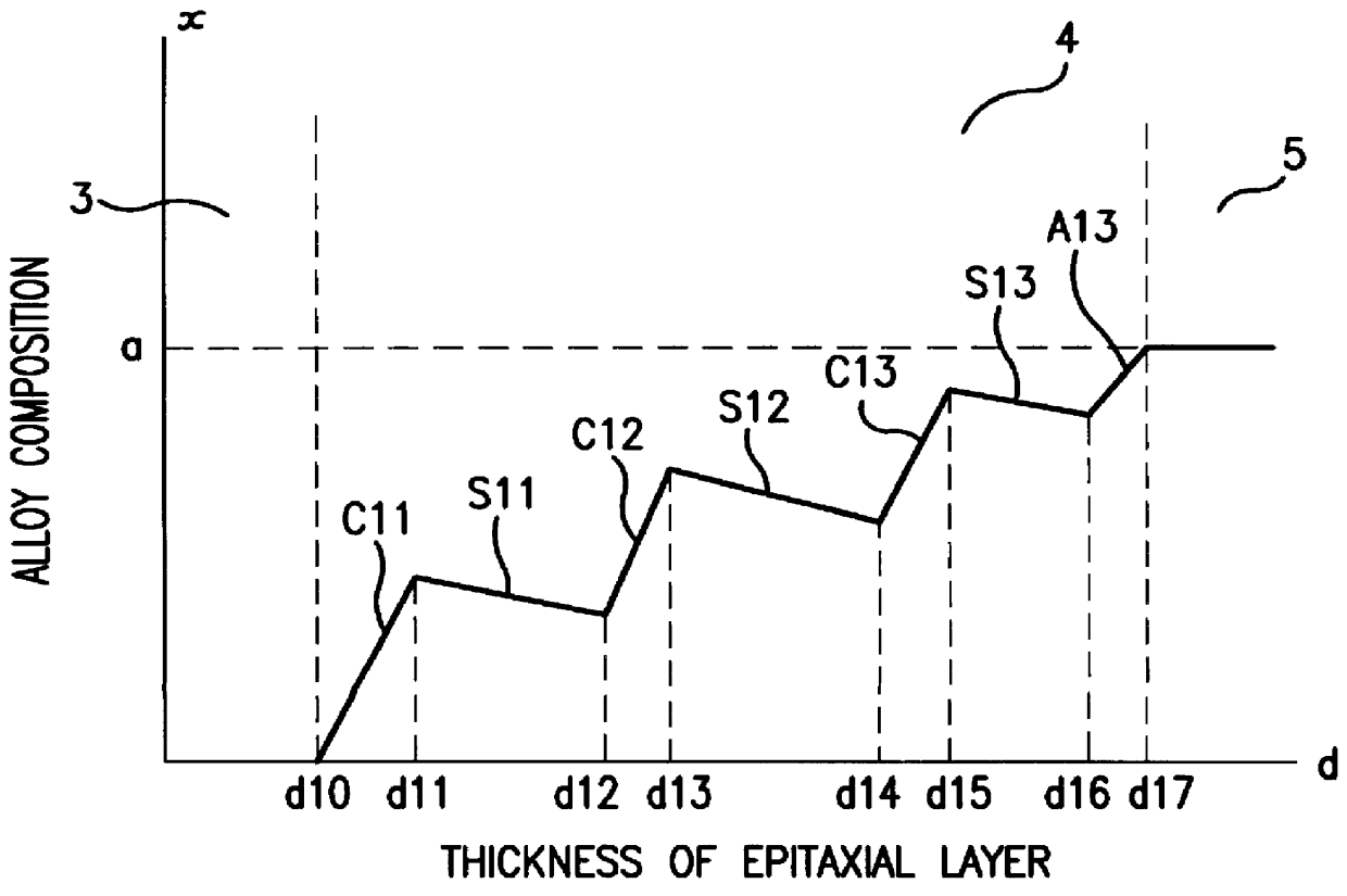
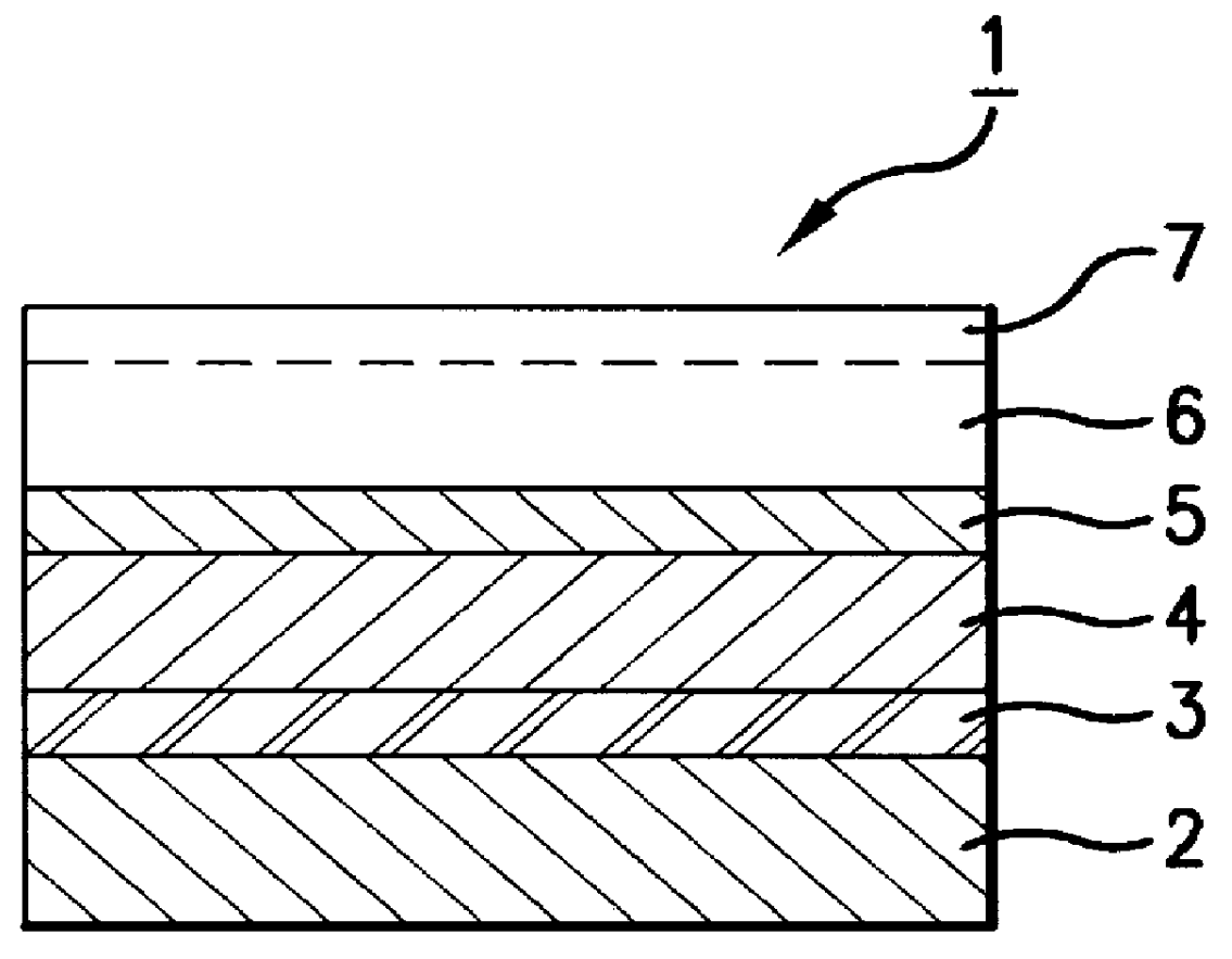
Fabricated in such a manner as will be explained below, was a GaAs.sub.a P.sub.1-a epitaxial wafer 1 for orange-color light emitting diode with a composition constant layer having an alloy composition a of 0.34.

A gallium phosphide GaP single crystal was cut into slices having a predetermined thickness, one of which was then subjected to a chemical etching process and a mechano-chemical polishing process to form a gallium phosphide GaP mirror-polished wafer having a thickness of about 300 .mu.m, and the wafer was used as a substrate 2. Used as reaction gases were a hydrogen H.sub.2 gas, a 50--ppm hydrogen sulfide H.sub.2 S gas diluted with hydrogen, a 10% arsine (hydrogen arsenide AsH.sub.3) gas diluted with hydrogen, a 10% phosphine (hydrogen phosphide PH.sub.3) gas diluted with hydrogen, a high purity hydrogen chloride HCl gas and a high purity ammonia NH.sub.3 gas.

First, the gallium phosphide GaP single-crystalline substrate 2 of an n type having a diameter of 50 mm, a crystal ori...


PUM

PropertyMeasurementUnit
thicknessaaaaaaaaaa
thicknessaaaaaaaaaa
thicknessaaaaaaaaaa

Abstract

PCT No. PCT / JP97 / 00050 Sec. 371 Date Oct. 21, 1998 Sec. 102(e) Date Oct. 21, 1998 PCT Filed Jan. 13, 1997 PCT Pub. No. WO97 / 25747 PCT Pub. Date Jul. 17, 1997At the time of forming an alloy composition gradient layer 4 of gallium arsenide phosphide GaAsxP1-x having an arsenic alloy composition x changed in such a range as not to exceed a predetermined alloy composition a with an increase of a layer thickness d between a GaP layer 3 and a composition constant layer 5 of gallium arsenide phosphide GaAsaP1-a having the predetermined alloy composition a to be grown above the GaP layer; the alloy composition x is abruptly ascended as in composition ascending zones C11 to C13 with the ascended thickness d of an epitaxial layer and then descended as in crystal stabilizing zones S11 to S13 in such a range as not to cancel the previous ascent amount. One or more combinations of such ascent and descent in the alloy composition are repeated to form as distributed in the alloy composition gradient layer 4, and then the alloy composition x is ascended to the predetermined alloy composition a. Thereby there is obtained a compound semiconductor epitaxial wafer which can effectively eliminate stresses caused by lattice mismatching, can be made thinner with an excellent productivity, and can have a high luminance due to employment of a reflective layer.

Description

This invention relates to a compound semiconductor epitaxial wafer and method for fabricating the wafer and more particularly, to a compound semiconductor epitaxial wafer containing gallium arsenide phosphide GaAs.sub.z P.sub.1-z (where 0.ltoreq.z.ltoreq.1) having a predetermined alloy composition.In red-, orange- and yellow-color light emitting diodes, there has been conventionally employed an epitaxial wafer in which an epitaxial layer of gallium arsenide phosphide GaAs.sub.z P.sub.1-z (where 0.ltoreq.z.ltoreq.1) is formed on a single-crystalline substrate of gallium phosphide GaP or gallium arsenide GaAs.When a lattice mismatching between the single crystal of the substrate of gallium phosphide GaP or gallium arsenide GaAs and the GaAs.sub.z P.sub.1-z epitaxial layer having an alloy composition formed on the substrate is large, this causes a misfit dislocation to take place at its interface, whereby a stress caused by the lattice mismatching is relaxed. When this dislocation prop...

Claims


Application Information

Patent Timeline
Patent Type & Authority Patents(United States)
IPC IPC(8): H01L33/00H01L21/20H01L21/203H01L21/205H01L33/30
CPCH01L33/30H01L33/12H01L33/00
Inventor WATANABE, MASATAKAKAISE, TSUNEYUKISHINOHARA, MASAYUKIENDOU, MASAHISATAKAHASHI, TOHRU
Owner SHIN-ETSU HANDOTAI CO LTD
Why Eureka
Try Eureka