Method for dual gate oxide dual workfunction CMOS

a dual work function, dual gate oxide technology, applied in the direction of transistors, semiconductor devices, electrical equipment, etc., can solve the problems of inability to achieve the dual work function of the dual gate oxide, the logic becomes prohibitively slow, and the voltage increases the electric field

Inactive Publication Date: 2000-07-11
GOOGLE LLC
View PDF15 Cites 93 Cited by
  • Summary
  • Abstract
  • Description
  • Claims
  • Application Information

AI Technical Summary

Problems solved by technology

However, boosting wordline voltage increases the electric field across the gate dielectric of transfer devices tied to the wordline.
For a typical DRAM chip with a uniform gate oxide thickness, the thickened gate oxide degrades performance in peripheral circuits and input/output (I/O) circuits.
While this degradation may cause an acceptable impact in DRAM performance, when a DRAM is merged with high performance logic, the logic becomes prohibitively slow.
There is, therefore, some reluctance in merging high performance logic with DRAM cells on a single chip, because of the inherent increase in process complexity.
Another problem is transient voltage spikes on I/O device gate oxide from I/O voltage overshoots and undershoots.
These decoupling structures occupy additional...

Method used


Image

  • Method for dual gate oxide dual workfunction CMOS
  • Method for dual gate oxide dual workfunction CMOS
  • Method for dual gate oxide dual workfunction CMOS

Examples


Embodiment Construction

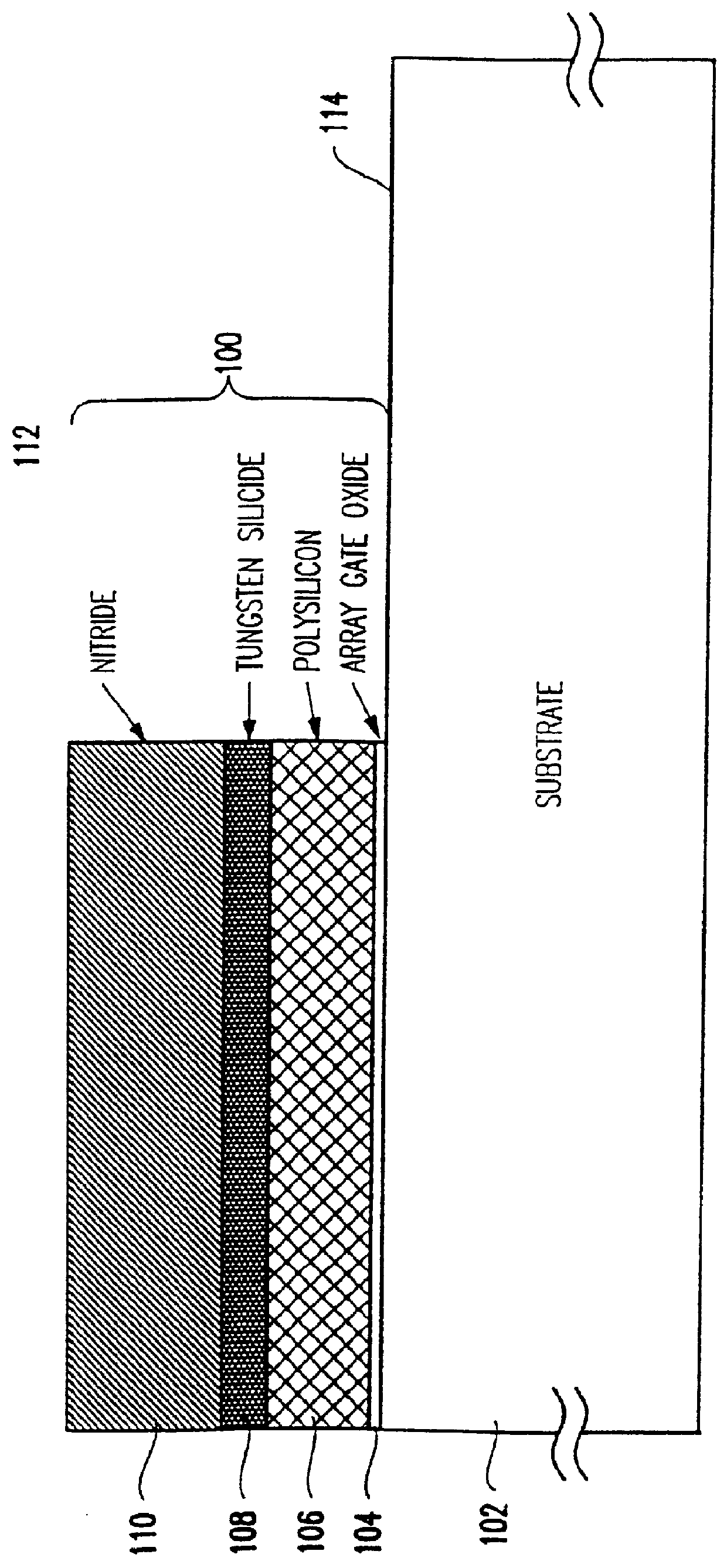
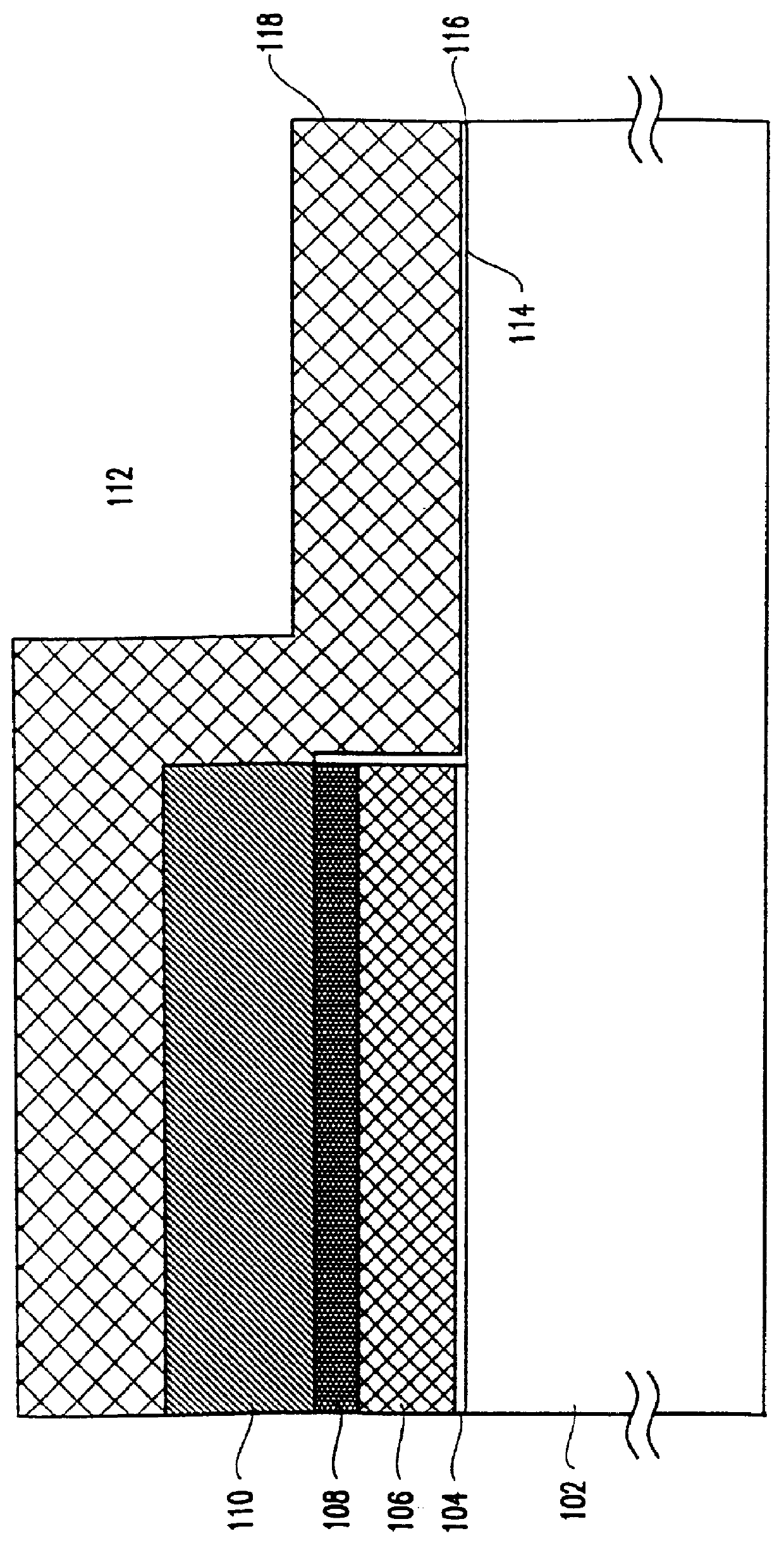
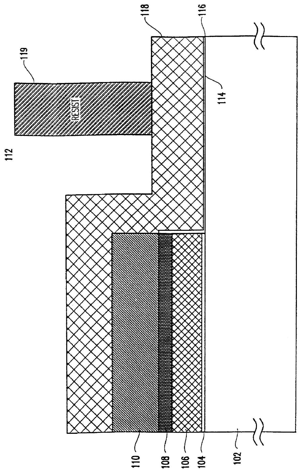
Referring now to the drawings, and more particularly to FIG. 1, which shows a first gate stack 100 formed according to the preferred embodiment of the present invention. The preferred embodiment of the present invention is a method of forming integrated circuit (IC) chips with multiple device types normally found on separate IC chips.

For example, a preferred IC device may include dynamic random access memory (DRAM) cells formed with DRAM specific process features and a high performance microprocessor formed for according to a logic process. The two processes are sufficiently decoupled to allow inclusion in either features specifically directed to the needs of the particular type device being formed. Thus, IC chips formed according to the preferred embodiment are formed using, effectively, two processes on the same chip.

As described herein for illustration, the first type devices, for DRAM, are formed from the first gate stack 100 in what is referred to herein as thick oxide areas. T...


PUM


Abstract

A method of forming integrated circuit chips including two dissimilar type NFETs and/or two dissimilar type PFETs on the same chip, such as both thick and thin gate oxide FETs. A DRAM array may be constructed of the thick oxide FETs and logic circuits may be constructed of the thin oxide FETs on the same chip. First, a gate stack including a first, thick gate SiO2 layer is formed on a wafer. The stack includes a doped polysilicon layer on the gate oxide layer, a silicide layer on the polysilicon layer and a nitride layer on the silicide layer. Part of the stack is selectively removed to re-expose the wafer where logic circuits are to be formed. A thinner gate oxide layer is formed on the re-exposed wafer. Next, gates are formed on the thinner gate oxide layer and thin oxide NFETs and PFETs are formed at the gates. After selectively siliciding thin oxide device regions, gates are etched from the stack in the thick oxide device regions. Finally, source and drain regions are implanted and diffused for the thick gate oxide devices.

Description

1. Field of the InventionThe present invention generally relates to semiconductor chip manufacturing processes and more particularly to dual gate oxide, dual work function field effect transistor manufacturing processes that may be adapted for manufacturing merged logic and dynamic random access memory chips.2. Background DescriptionDynamic random access memory (DRAMs) and logic designs have different design points and requirements. Logic design is focused, typically, on speed at the cost of increased power. Consequently, high device leakage current can be tolerated. By contrast, the primary focus in DRAM design is minimizing leakage currents that would otherwise reduce memory cell data retention time.State of the art IC chips must be able to allow wider ranges of on-chip voltages, while increasing circuit performance and design flexibility.For example in DRAM designs, it is necessary to boost the wordline voltage above the circuit power supply voltage to increase the charge stored ...

Claims


Application Information

Patent Timeline
IPC IPC(8): H01L21/8242H01L21/70H01L21/8238H01L21/8234H01L27/088H01L27/10H01L27/108
CPCH01L21/823842H01L27/10873H10B12/05H01L21/8232
Inventor BRONNER, GARY BELAEL-KAREH, BADIHSCHUSTER, STANLEY EVERETT
Owner GOOGLE LLC
Why Eureka
Try Eureka