Multi-element deflection aberration correction for electron beam lithography

a lithography and electron beam technology, applied in the direction of beam deviation/focusing, magnetic discharge control, instruments, etc., can solve the problems of inability to realistically approach the problem of reducing only viable e-beam exposure, and inability to reduce the exposure time of the sho

Inactive Publication Date: 2001-01-30
NIKON CORP
View PDF8 Cites 62 Cited by
  • Summary
  • Abstract
  • Description
  • Claims
  • Application Information

AI Technical Summary

Benefits of technology

It is another object of the invention to provide an arrangement of optical elements which can provide adjustment of focus and simultaneous compensation of magnification and, if magnetic elements are used, rotation.
It is a further object of the invention to provide control of optical elements which can achieve focus adjustment without causing sub-field magnification change and rotation.
It is a further object of the invention to provide an arrangement of optical elements which can provide substantially independent correction of FSD and SFD.

Problems solved by technology

However, it can be appreciated that e-beam exposure is only viable as an exposure medium for high volume production of integrated circuits (ICs) if a throughput comparable to EMR exposure techniques such as DUVL can be realized.
Therefore, a very large number of sequential exposures is required to make an exposure of a complete chip area pattern and throughput of probe-forming systems is unacceptably low.
This problem cannot realistically be approached by reduction of shot exposure time in view of the large number of exposures which must still be made.
However, exposure of such an extensive area is not currently practical for various reasons including distortion and field curvature of the electron-optical system (which are correctable to tolerable residual error over only small areas) and available flatness of a wafer surface over a chip area.
However, such systems have not heretofore been successfully applied to minimum feature sizes approaching or below one-tenth micron and in which the pattern may include one million pixels or more.
That is, the beam size and orientation error which results from magnification change or rotation over the small beam transverse dimension will be a tolerably small fraction of the beam size.
The same is not true for a LARPO system in which correction is substantially more complicated.
Further, correction of either type of distortion may affect the magnitude of the other.
Similarly, changes in magnification and rotation of the image cannot be ignored when the sub-field size is much larger than the feature size.
In LARPO systems utilizing curvilinear variable axis lenses (CVAL), as described in U.S. Pat. No. 5,635,719, which is hereby fully incorporated by reference, additional complexity arises from the superposition of focusing and deflection fields leading to aberrations referred to as "hybrid".
However, while such a minimum of optical elements may be sufficient, in principle, to achieve such corrections, no practical embodiment is suggested by Hosokawa et al.
Therefore, accepted theory of charged particle optics provides no guidance concerning the location of multiple astigmatism and focus correction elements.
However, it should be recognized that there has been no practical solution to correction of both feature shape and sub-field distortion and / or correction of field curvature while minimizing both image rotation and magnification change, even though practical electron and ion beam devices, the theory of operation and electromagnetic beam control therein and the interaction of correction of types of astigmatism and field curvature has been known for many years.

Method used


Image

  • Multi-element deflection aberration correction for electron beam lithography
  • Multi-element deflection aberration correction for electron beam lithography
  • Multi-element deflection aberration correction for electron beam lithography

Examples


Embodiment Construction

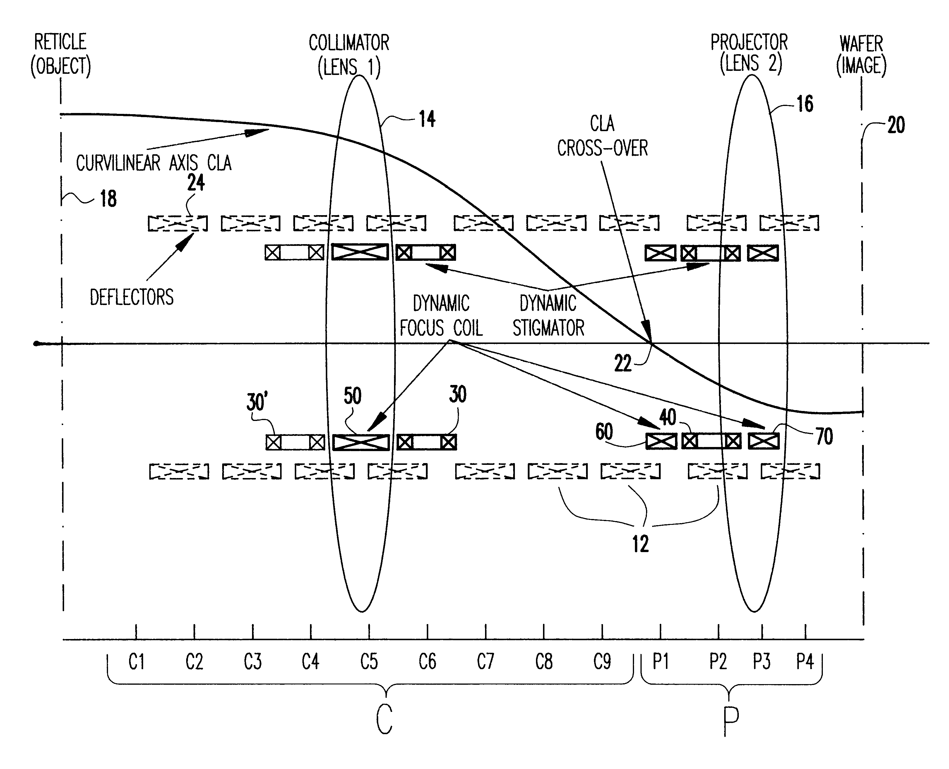
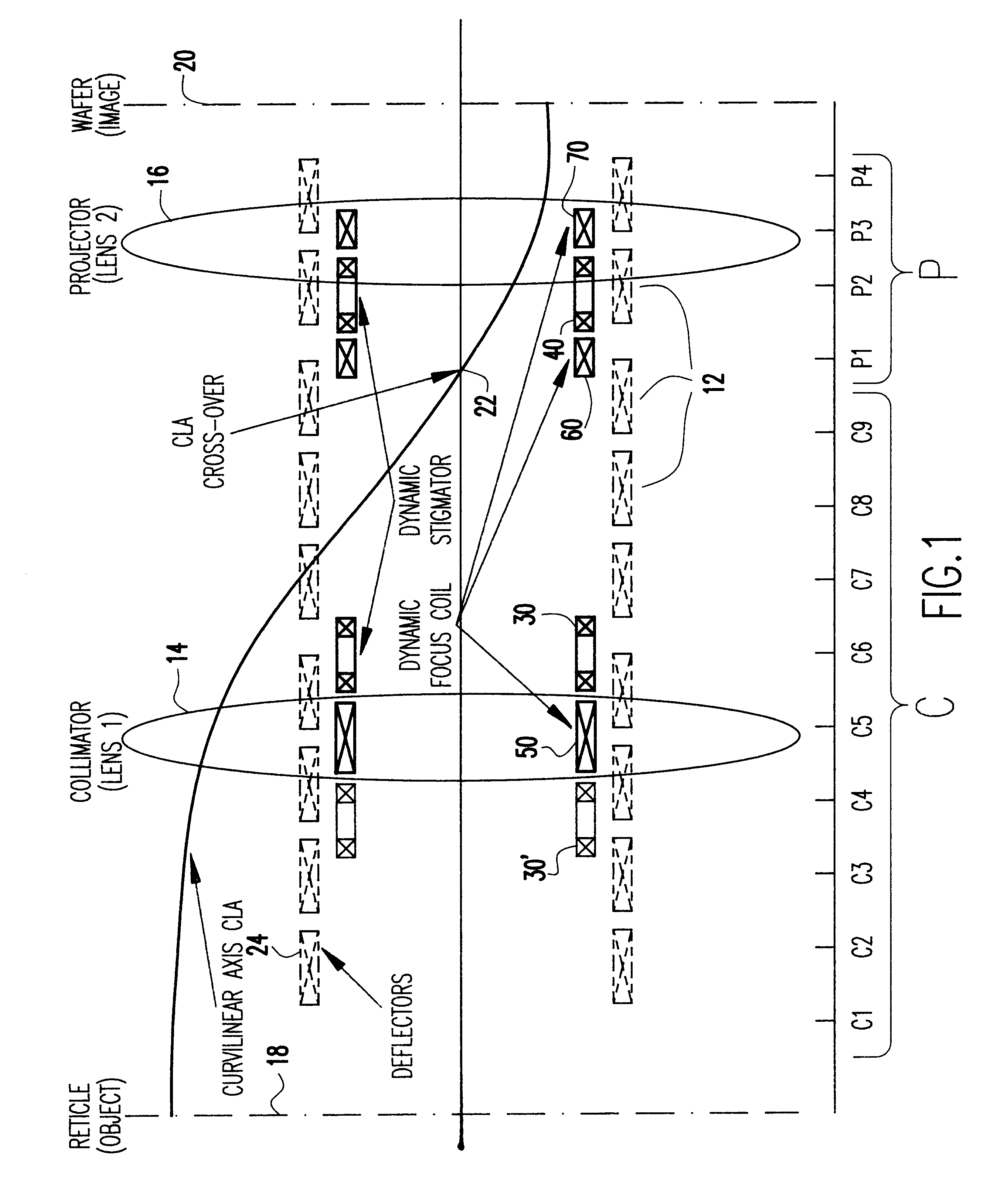
Referring now to the drawings, and more particularly to FIG. 1, there is shown a schematic, cross-sectional view of the reticle imaging optics with key elements of an e-beam projection system employing LARPO and CVAL optics. Elements of the system which are not important to an understanding of the invention, including the remainder of the e-beam column, are omitted in the interest of clarity. Elements illustrated with dashed lines are schematic depictions of coils 12 forming deflectors of the e-beam projection system with which the invention is employed. Distributed lenses of the system are schematically depicted at 14, 16. These coils and lenses are not drawn to scale in size or location and do not specifically depict any particular e-beam projection system. Accordingly, no portion of FIG. 1 or any other Figure in the application is admitted to be prior art in regard to the present invention.

The reticle imaging optics of FIG. 1 are generally divided into a collimator section C and ...


PUM

PropertyMeasurementUnit
feature sizesaaaaaaaaaa
sizeaaaaaaaaaa
sizesaaaaaaaaaa

Abstract

A method of optimizing locations of correction elements of a charged particle beam system determines respective corrector element currents to achieve optimum correction as a function of individual corrector location. Substantially complete dynamic correction of FSD and SFD can be obtained consistent with efficiency of operation and minimization of deflection distortion. In particular, FSD and SFD corrections can be sufficiently separated for substantially complete correction of SFD and FSD simultaneously with two stigmators. Both of these types of correction can be provided in complex charged particle beam systems employing curvilinear axis (CVA) particle trajectories and or large area reduction projection optics (LARPO) which cause complex hybrid aberrations in order to achieve high throughput consistent with extremely high resolution supporting one-tenth micron minimum feature size lithography regimes and smaller.

Description

1. Field of the InventionThe present invention generally relates to optical correction of charged particle beam tools and, more particularly, to reduction and compensation of aberrations in electron beam (e-beam) projection systems.2. Description of the Prior ArtNumerous techniques are known utilizing charged particle beams and are in widespread use for manufacture of integrated circuit devices, in particular. For example, charged particle beams are used for implantation of impurities, inspection (e.g. with scanning electron microscopes) of structures for process evaluation and development and for lithographic patterning of substrates and layers deposited thereon.Essentially, lithography processes define potentially very minute areas and shapes on a surface through selective exposure and removal of portions of a layer of resist to expose areas of the surface for further processing by, for example, etching, implantation and / or deposition. In general, for semiconductor device manufact...

Claims


Application Information

Patent Timeline
Patent Type & Authority Patents(United States)
IPC IPC(8): H01J37/153H01J37/04H01J37/304H01J37/30H01L21/027G03F7/20
CPCH01J37/153H01J37/304H01J2237/3045H01J2237/3175
Inventor STICKEL, WERNERGORDON, MICHAEL S.PFEIFFER, HANS C.GOLLADAY, STEVEN D.
Owner NIKON CORP
Why Eureka
Try Eureka