

Organic electroluminescent device
a technology of electroluminescent devices and electroluminescent light, which is applied in the direction of discharge tubes/lamp details, discharge tubes luminescnet screens, electric discharge lamps, etc., can solve the problems of reduced device life, poor hole blockage of silicon monoxide (sio), and difficulty in achieving efficient recombination of electrons with holes in the light emitting layer, etc., to achieve high efficiency, long life, and high stability.
- Summary
- Abstract
- Description
- Claims
- Application Information
AI Technical Summary
Benefits of technology
Problems solved by technology
Method used
Image

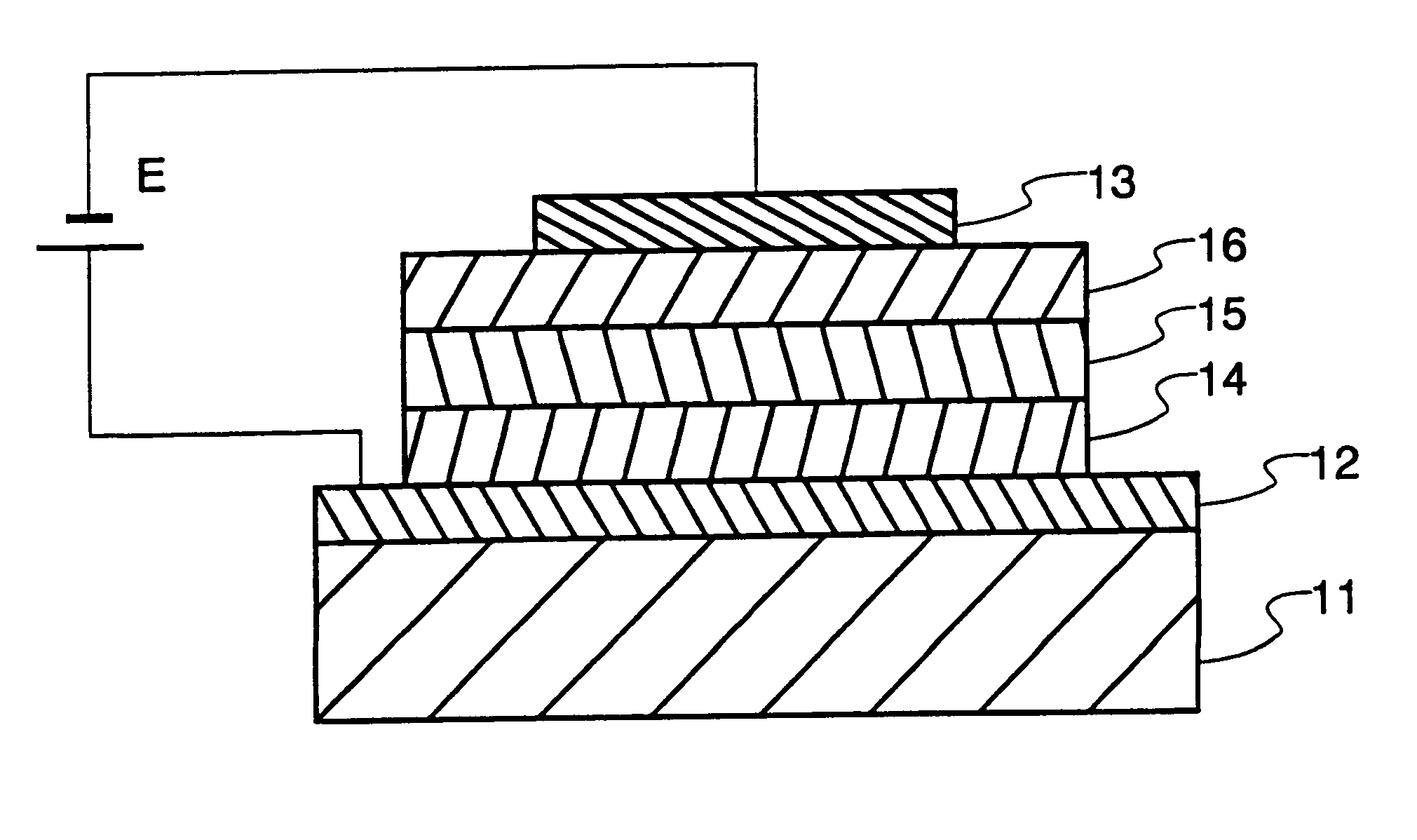
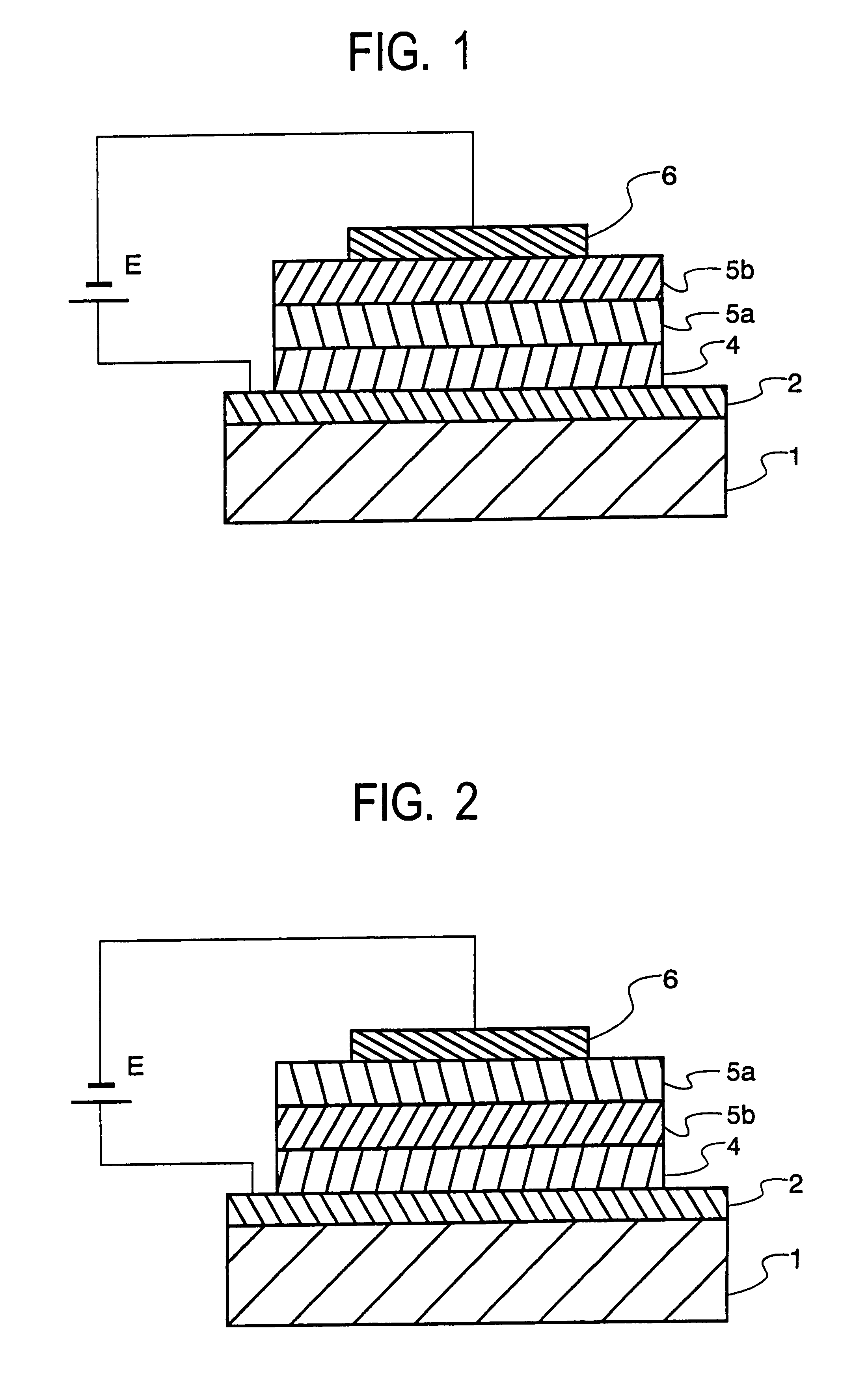
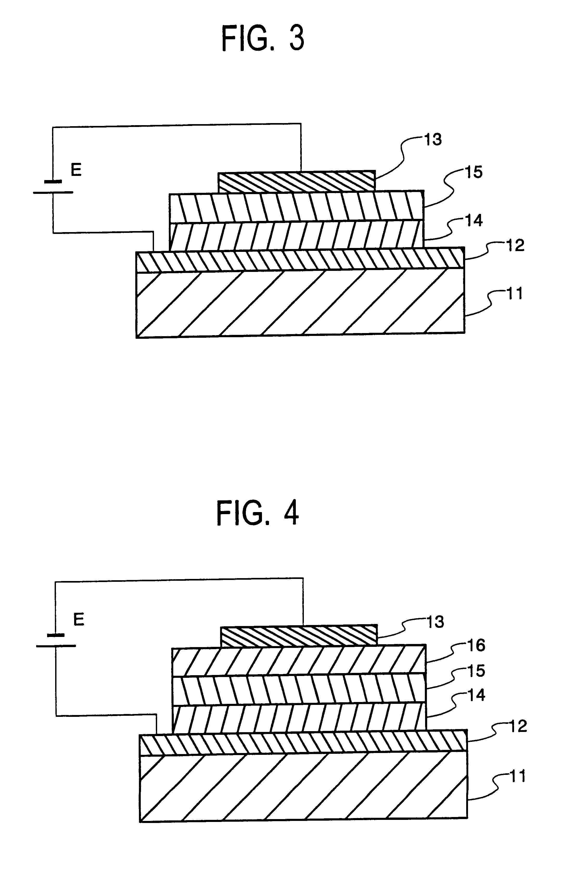
Examples
example 1
A substrate of (7059) glass by Corning Glass Works was scrubbed using a neutral detergent.
By RF magnetron sputtering from a target of ITO oxide, a hole injecting electrode layer of ITO having a thickness of 200 nm was formed on the substrate at a temperature of 250.degree. C.
After its ITO electrode-bearing surface was cleaned with UV / O.sub.3, the substrate was secured by a holder in a vacuum deposition chamber, which was evacuated to a vacuum of 1.times.10.sup.-4 Pa or lower.
Next, using a target of SiO.sub.2, an inorganic insulative hole injecting and transporting layer was deposited to a thickness of 2 nm. The sputtering gas used was a mixture of argon and 5% of oxygen (O.sub.2). Sputtering conditions included a substrate temperature of 25.degree. C., a deposition rate of 1 nm / min, an operating pressure of 0.5 Pa, and an input power of 5 W / cm.sup.2. The inorganic insulative hole injecting and transporting layer as deposited had a composition of SiO.sub.1.9.
With the vacuum kept, tri...
example 2
In Example 1, the main component and stabilizer of the inorganic insulative electron injecting and transporting layer were changed from Li.sub.2 O to K.sub.2 O, Rb.sub.2 O, K.sub.2 O, Na.sub.2 O, Cs.sub.2 O, SrO, MgO, CaO or mixtures of these oxides, and from SiO.sub.2 to GeO.sub.2 or oxide mixtures of SiO.sub.2 and GeO.sub.2, respectively, with substantially equivalent results.
example 3
An organic EL device was fabricated as in Example 1 except that the inorganic insulative electron injecting and transporting layer had the composition consisting of strontium oxide (SrO), lithium oxide (Li.sub.2 O), and silicon oxide (SiO.sub.2) in the proportion:
SrO:35 mol %,
Li.sub.2 O:60 mol %
SiO.sub.2 :5 mol %,
based on the entire components. The thus obtained organic EL device was tested as in Example 1, finding substantially equivalent results. Substantially equivalent results were obtained from other combinations of alkali metal elements with alkaline earth metal elements.
PUM
 Abstract
Description
Claims
Application Information