In recent years, high integration of semiconductor integrated circuit elements considerably increases and there is a tendency to increase markedly the heating value during the operation of the semiconductor element, so it becomes an important problem to rapidly release heat generated by the semiconductor integrated circuits outside of the semiconductor device in order to prevent abnormal operation of the element arising from overheating.
As a result, it is afraid that the thermally conductive compound might be destroyed or the semiconductor integrated circuit might be destroyed by a reaction, or cracks or peeling-off might be produced at the surface of the thermally conductive compound with the circuit element or cap.
Accordingly, a variety of thermally conductive compounds and semiconductor devices have been proposed because the merely high
thermal conductivity is insufficient.
The semiconductor device as proposed in JP-A 61-29162 (1986) has such a problem that the
silicon gel as a thermally conductive material, which usually has a low
thermal conductivity of approximately 0.2-0.3 W / mK, insufficiently transfers heat to probably overheat the semiconductor integrated circuit elements when used as
heat transfer means for the current semiconductor integrated circuit elements of which the calorific value strikingly increases.
Moreover, it was also problem that since the
viscosity of
silicon gel is high, when the filler is intended to charge at a
high rate, there is formed cracks in the filler because of insufficient distribution of the
silicon gel so that the thermal
conductivity of the thermal conductive material cannot be increased sufficiently.
On the other hand, in the integrated circuit
package proposed in Japanese Unexamined Patent Publication JP-A 61-36961 (1986), it was problem that since the integrated circuit
chip and the
radiation plate are adhered with a thermally conductive
adhesive, when the coefficient of
thermal expansion is considerably different between both materials, mechanical stress due to the
temperature difference of both materials is exerted on the integrated circuit chips possibly causing destruction, so the coefficient of
thermal expansion of the
radiation plate is required to be equal to that of the integrated circuit chips, the choices of the material of radiation plate is limited, and the radiation plate cannot be produced with a material having high thermal
conductivity.
It was a problem, however, that when a method for
chip disposition other than the TAB method is employed, for example, when the
chip is mounted on the substrate through a solder layer by a flip-chip mounting, the use of this radiation structure causes destruction of the solder layer with vertical or horizontal movement of the chip body and the connection of the integrated circuit with the substrate cannot be maintained.
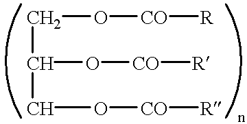
On the other hand, the thermally conductive compounds proposed in Japanese Examined Patent Publication JP-B2 6-95557 (1994) are
grease-like thermally conductive compounds prepared by dispersing thermally conductive filler particles in an organic liquid as a carrier, and when the compounds are used as thermally
conductive materials in a semiconductor device,
moisture contained in an airtight sealed-up cavity sometimes acts on the binder contained in the thermally conductive compounds to join together; as a result, there is a fear that the capacity of the thermally conductive filler particles becomes insufficient and cause phase separation between the organic liquid as carrier and the thermally conductive filler particles.
As a result of the phase separation, the organic liquid flows out to cause shortage of amount and to form cavities of flowing-out, which disturb
heat transfer or produce aggregate of the thermally conductive filler particles making the heat transfer uneven in the thermally conductive compounds or causing decrease of
mechanical strength of the thermally conductive filler particles such as falling-off of the thermally conductive filler particles.
When the rate of the carrier resin in the thermally conductive compound is lower than 15 volume % (the filler particles over 85 volume %), it becomes difficult to link together and maintain the filler particles which are in contact with each other forming a thermally conductive
route because the amount of the carrier resin is insufficient for that of the filler particles, and so it becomes a problem that part of the filler particles are not involved in linkage and
mechanical strength of the thermally conductive compound in a form of sheet decreases, and further it becomes difficult to make the surface of the thermally conductive compound smooth because the part of the filler particles protrude from the surface of the thermally conductive compound due to lack of the carrier resin.
As a result, it might be difficult to make the thermal
conductivity of the compound higher than 1 W / m K.
Accordingly, even in the case where the thermally conductive compound prepared with the carrier resin is used as heat transfer means between an element and an insulator body or cap in a semiconductor device and the device has to be heated up to about 200-250.degree. C. in a
reflow oven in installing the semiconductor device in an
external circuit with a solder, in order to fuse the solder, the carrier resin is not thermally decomposed to effectively keep the function as heat transfer means.
The amount of the dispersing agent to be added, when it is lower than 0.5 weight % to the filler particles, is in-sufficient for homogeneously dispersing all of the filler particles into the carrier resin, and the filler particles which have not reacted with the dispersing agent are aggregated and unevenly distributed in the thermally conductive compound; as a result, the thermal conductivity of the thermally conductive compound becomes uneven and, at the portion at which the filler particles are unevenly distributed, the
mechanical strength is decreased due to lack of the carrier resin.
On the other hand, even though the dispersing agent was added at a rate of higher than 5 weight % to the filler particles, the dispersing effect of the filler particles could not be improved and rather the semiconductor device might receive a bad influence from the excess amount of the dispersing agent further added; particularly, in the case of the thermally conductive compound in which the mixing rate of the filler particles is high, there is a tendency to have a bad influence more often because a much more amount of the dispersing agent have to be added.
The heat conduction on the surface, however, is inferior to that inside of the filler particles, and therefore, it becomes difficult to enhance the thermal conductivity of the thermally conductive compound up to 1 W / m.multidot.K or more.
In view of the form of the thermally conductive compound in using, wherein the compound interposed between both the parts works to transfer heat from one to the other, when the particle size exceeds the distance between both the parts, namely, the thickness of the thermally conductive compound in using, there is a possibility that the filler particles protrude on the surface of the thermally conductive compound to spoil smoothness of the surface and disturb adhesion of the thermally conductive compound to both the parts.

