The
electronic switch of the present invention, in one realization, is a
quantum-state
molecular switch comprising an electrically adjustable
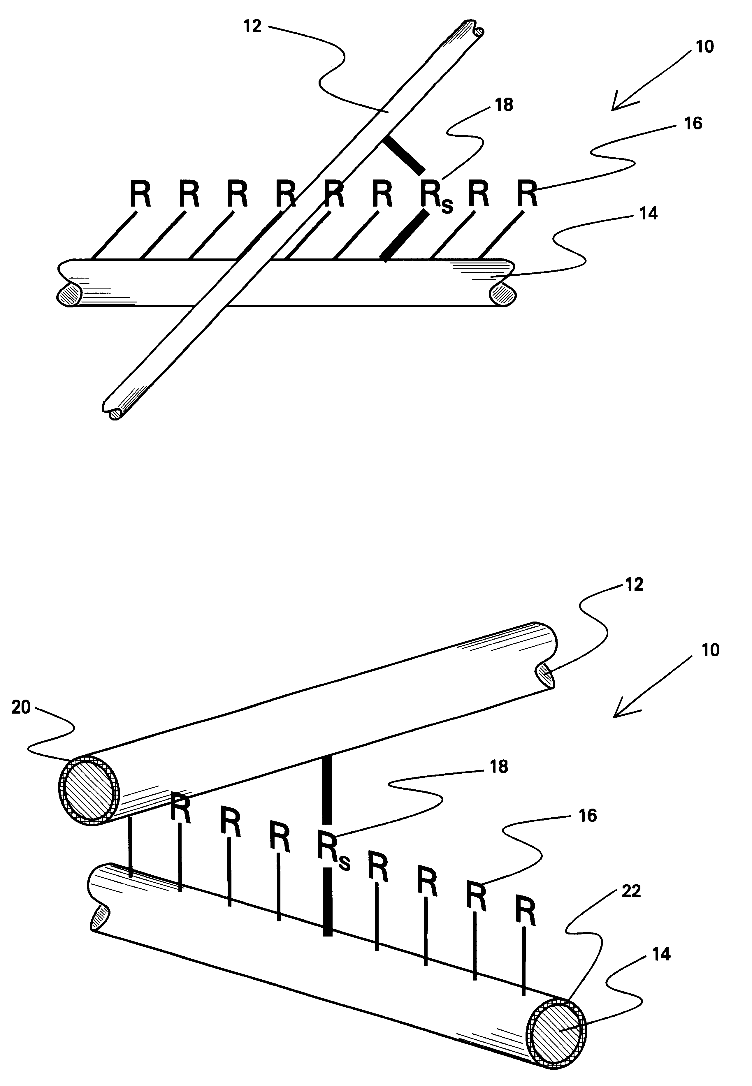
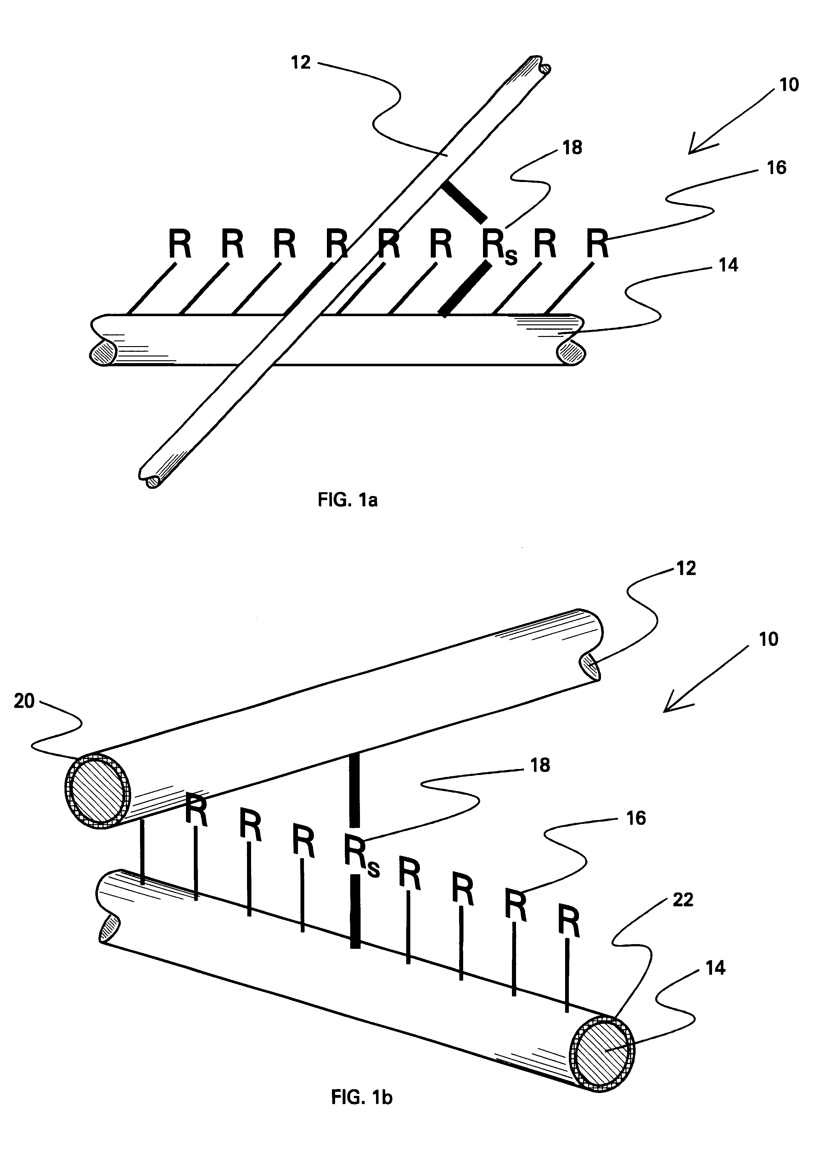
tunnel junction between two wires. Only at the intersection of the two wires is an actual device defined. The exact position of this intersection is not important for this architecture. The molecular devices sandwiched between the wires can be electrochemically oxidized or reduced. Oxidation or reduction of the molecule forms the basis of a switch. Oxidation or reduction will effect the tunneling distance or the tunneling barrier height between the two wires, thereby exponentially altering the rate of charge transport across the wire junction. Some types of molecules can be cycled reversibly (reconfigurable), while others will act irreversibly (singly configurable). The
chemical state of the molecular switches determines the tunneling resistance between the two wires. Each switch consists of two crossed wires sandwiching an electrically addressable molecular device. The approach is extremely simple and inexpensive to implement, and scales from wire dimensions of several micrometers down to nanometer-scale dimensions. This method requires only a set of bi-stable switches which can control electrical contact between the two
layers of wires approximately perpendicular to the two parallel planes defined by the crossbar wires (Z direction).
The above description is directed to controlling connections between
layers. Controlling connections within a layer are essential for realizing a practical crossbar. In order to create an arbitrary circuit from a highly ordered set of wires and switches such as a crossbar, it is necessary to make cuts at specific locations to break the electrical continuity along certain wires (in the plane of the crossbar). This enables functions in one part of the
regular array of wires and switches to be isolated from those of other parts, and in conjunction with open switches between the two
layers of a crossbar allows electrical signals from different finctions to be routed through each other without interfering. Given the fact that the crossbars described herein are made from junctions, which are essentially electrochemical cells, between sets of crossing wires, such cuts can be made by over-oxidizing a particular junction to consume a localized region of the wire to be
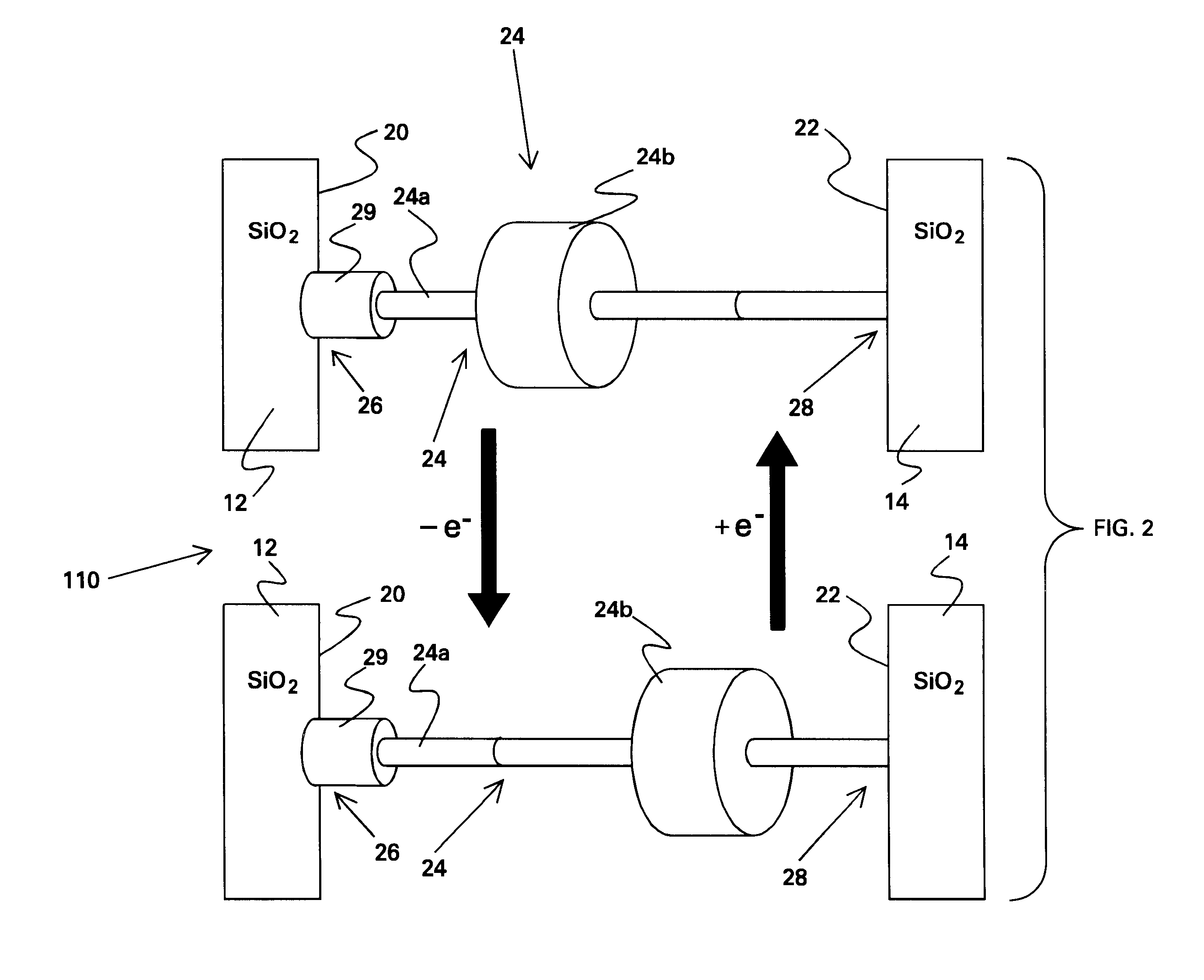
cut, and thus form an insulating gap that breaks the electrical continuity of that wire at the desired location. Thus, there are at least three different
voltage levels (which may be different magnitudes of the same polarity or involve different polarities) utilized in configuring a crossbar into a communications interconnect and using it. The first
voltage level is relatively large, and it is used only to over-oxidize a junction to create an electrical break in a wire. The next
voltage level is smaller in magnitude, and it is used to oxidize or reduce some or all of the molecules or materials between two wires to open or close a switch and thus disable or enable a particular type of connection between the wires in different levels of the crossbar. Finally, the third voltage is the smallest in magnitude, and that is the voltage level used to actually propagate information through the circuit. The three voltages must be separated enough from each other to avoid unintentional setting of switches or
cutting of wires by
signal propagation.
The
molecular wire crossbar switch and the
resultant crossbar network built from multiple sets of these switches allows the construction of an arbitrarily-designed logic circuit. All of the
interconnection required by that logic circuit is at a nanometer scale. In effect, all of the wiring required of a complex
integrated circuit can be created by this mechanism without the use of
lithography. The present invention enables construction of molecular electronic devices on a
length scale that can range from micrometers to nanometers via a straightforward and inexpensive chemical
assembly procedure. The device is either partially or completely chemically assembled, and the key to the scaling is that the location of the devices on the substrate are defined once the devices have been assembled, not prior to
assembly.
The primary
advantage of the present invention is ease of fabrication, because an
active switch is formed any time two wires cross. These switches, which are used to define the
interconnection topology of the
integrated circuit, are formed by a highly parallel
chemical process. This enables formation of trillions of switches in a time no longer than it takes to form thousands of switches.
A second advantage of the present invention is that it saves tremendously on circuit area (a factor of a few times ten), since no other wires or ancillary devices are needed to operate the switch or store the required configuration. This reduction of the area of a configuration bit and its switch to just the area of two crossing wires is a major advantage in constructing a defect tolerant interconnect network; see, U.S. Pat. No. 5,790,771, "Apparatus and Method for Configuring a Reconfigurable Electronic
System Having Defective Resources", issued to W. B. Culbertson et al on Aug. 4, 1998, and assigned to the same assignee as the present invention. If the area cost of defect tolerance substantially exceeds that of the interconnect used by the circuit, it becomes prohibitively expensive and the
area density advantages of a nanometer-sized technology are lost. The present invention (MWCI) has the major advantage that the increased efficiency in packing configuration bits reduces the cost of defect tolerance (making it essentially free in terms of circuit area) for precisely those components (molecular scale devices and wires) that might require defect tolerance in order to be used at all.
Finally, since only two wires are needed to address and set the switches which define the integrated circuit being constructed, and since the switch itself is defined not by
high resolution lithographic templating, but rather by the relatively arbitrary intersection of two wires, the fabrication process for these integrated circuits is substantially simpler and tolerant of manufacturing deficiencies than is the current art.

