Manufacturing method of a thin film on a substrate

Inactive Publication Date: 2002-11-26
FORMOSA SOI
View PDF2 Cites 240 Cited by
  • Summary
  • Abstract
  • Description
  • Claims
  • Application Information

AI Technical Summary

Problems solved by technology

However, the wafer bonding technology still has some disadvantages, such as the existence of the etch-stop layer on the surface of the wafer after etching and the uniformity of etching on different sites of the etch-stop layer caused the problem related to the total thickness variation (TTV).
In addition, the process requires too much time-not only many supply substrates are wasted, and some environmental pollution problems may occur due to the discarded fluid.
Because the thin film formed by SIMOX method has a perfect uniform thickness, wafer bonding technology may lost its leadership in the field of SOI wafer production if its TTV value can not be improved.
But the Smart-Cut process has some disadvantages, such as the thermal stresses generated from thermal treating process or the low manufacturing efficiency due to the time to reach sufficient strong bonding strength at lower temperature prior to layer splitting.
1. According to the low temperature bonding technology, the initial bonded wafer pairs need a long annealing time to enhance the bonding strength. That is, before the bonding strength is strong enough to gather bubbles to form a force to separate the wafers, the temperature must be controlled lower than 450.degree. C. which is the temperature that the hydrogen ions cause distinct bubbles. Because the initial bonded wafer pairs must be c

Method used


Image

  • Manufacturing method of a thin film on a substrate
  • Manufacturing method of a thin film on a substrate
  • Manufacturing method of a thin film on a substrate

Examples


Example

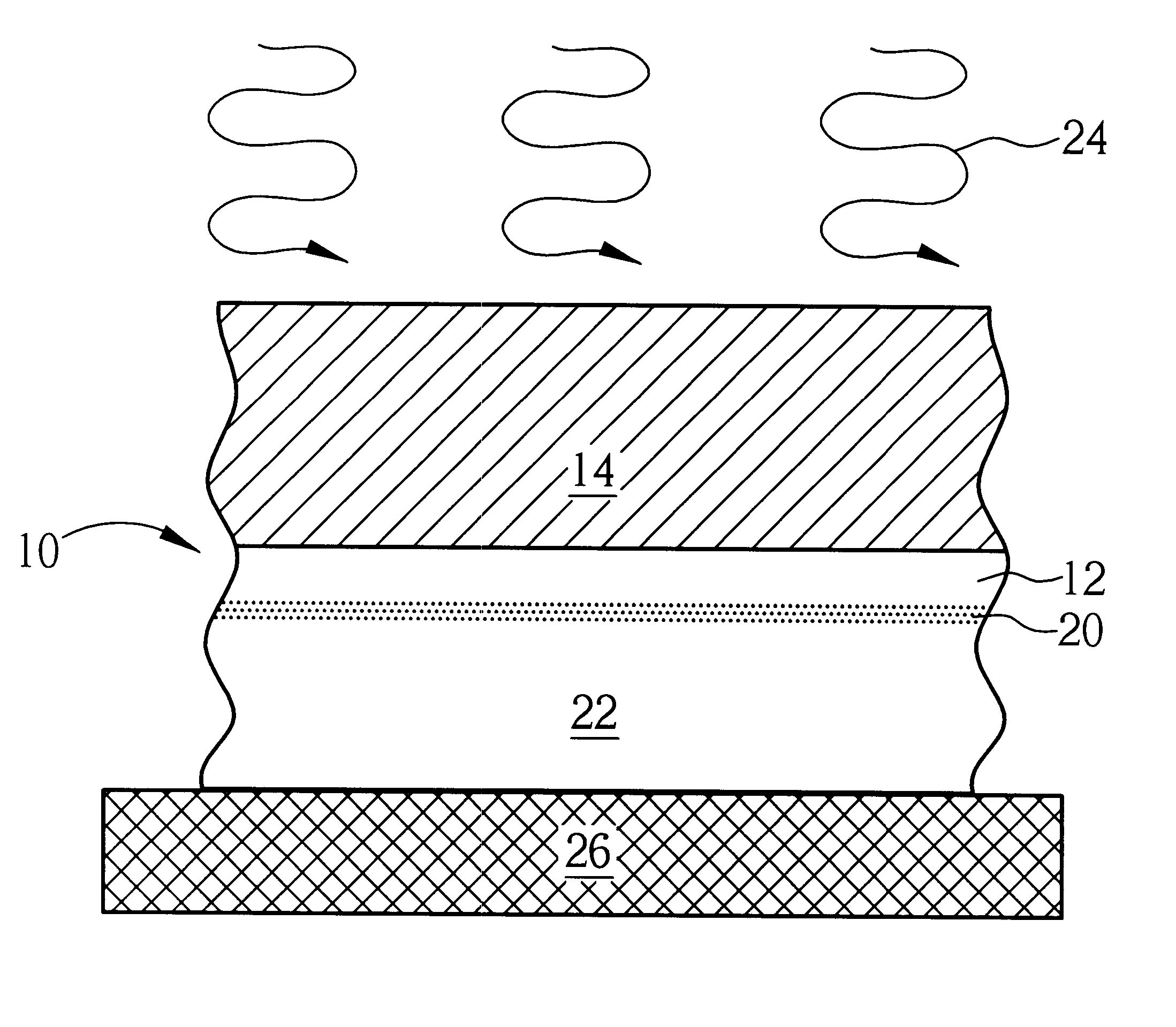
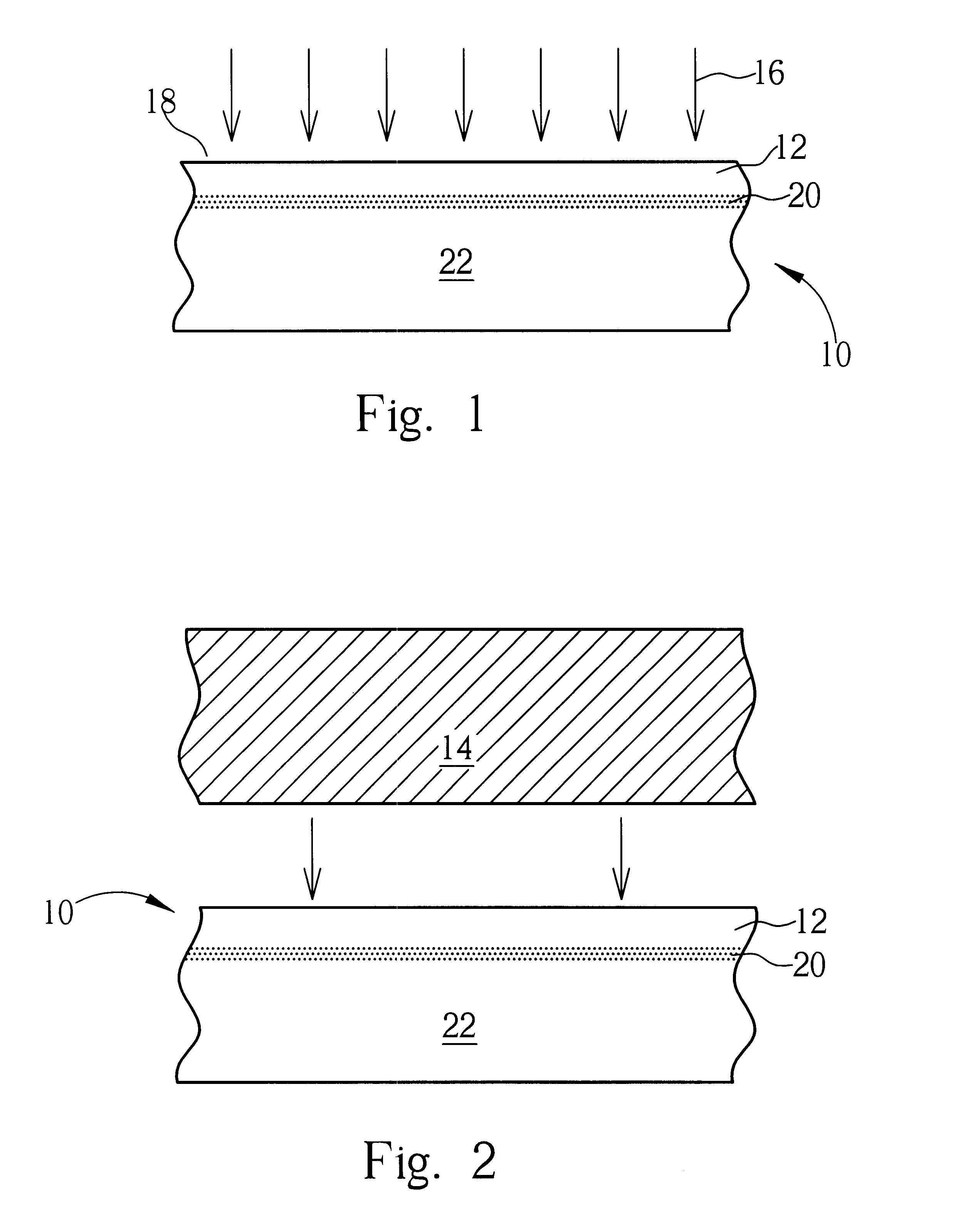
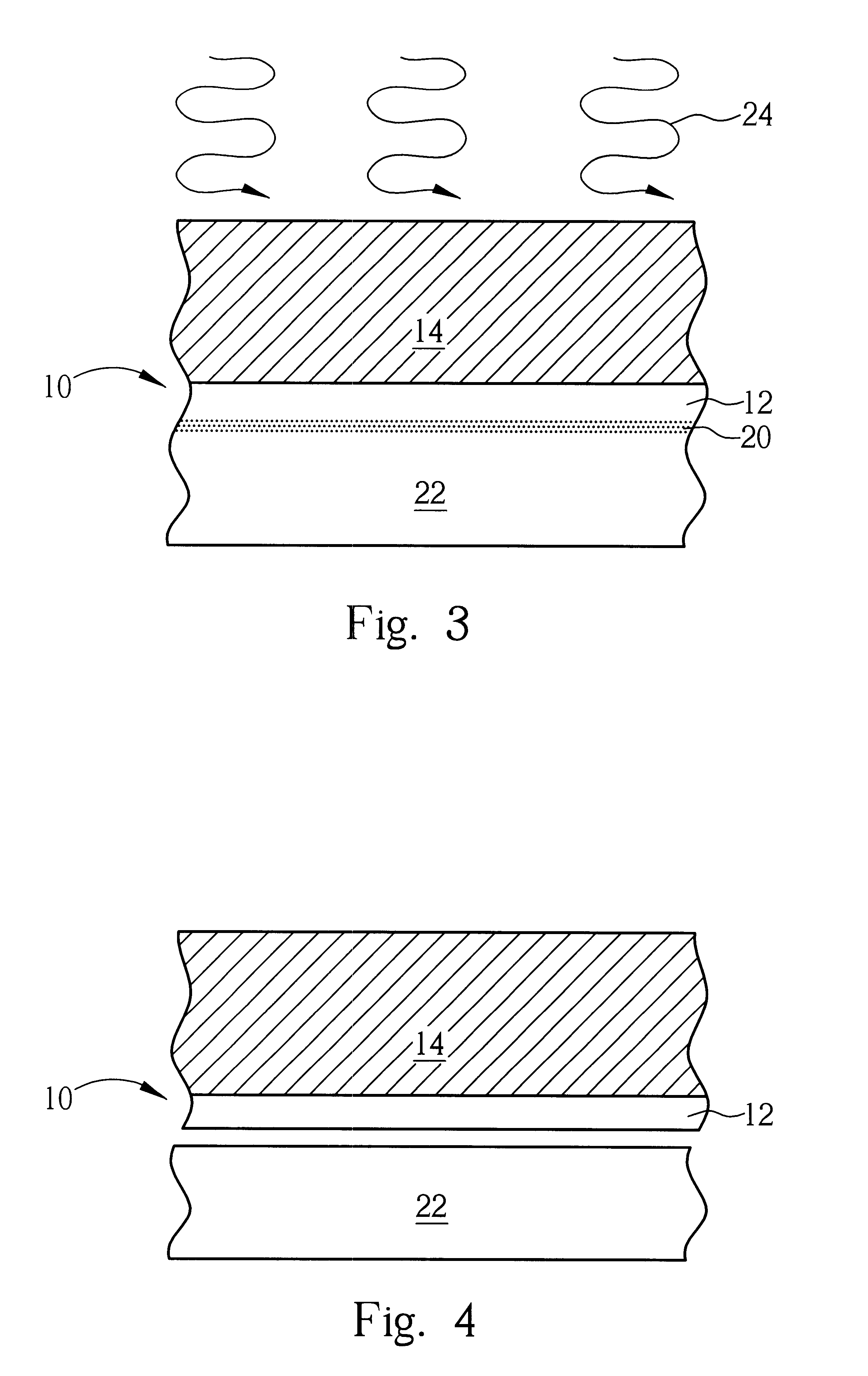
The first embodiment shows that the kinetic energy of the implanted ions or ionic molecules in the ion separation layer is excited with electromagnetic irradiation, in this case microwave irradiation, in achieving layer transfer.

In the first embodiment, the supply substrate is a p-type, one side polishing, (100), and 15-25 ohm-cm silicon wafer. The surface of the supply substrate is covered with silicon nitride (Si.sub.3 N.sub.4) of 1500 .ANG. thick and silicon dioxide of 500 .ANG. thick under the silicon nitride layer. 3.5.times.10.sup.16 atoms / cm.sup.2 of hydrogen ions with energy 200 KeV is implanted into the substrate. The demanded substrate is a p-type, one side polishing, (100), and 15-25 ohm-cm silicon wafer. The two wafers are bonded by low temperature wafer bonding method first and the bonded pair is placed in a microwave setup and irradiated at 2.45 GMz for five minutes. Then a silicon thin film of about 0.75 .mu.m thick is separated from the supply substrate and transferr...

Example

In the second embodiment, the supply substrate is a p-type, one side polishing, (100), and 15-25 ohm-cm silicon wafer. The surface of the supply substrate is covered with silicon nitride (Si.sub.3 N.sub.4) of 1500 .ANG. thick and silicon dioxide of 500 .ANG. thick under the silicon nitride layer. 3.5.times.10.sup.16 atoms / cm.sup.2 of hydrogen ions with energy 200 KeV is implanted into the supply substrate. The demanded substrate is a p-type, one side polishing, (100), and 15-25 ohm-cm silicon wafer. The two wafers are bonded by low temperature wafer bonding method first and the bonded pair is placed in a microwave setup with a cooler to keep the irradiating temperature no greater than 400.degree. C., and is irradiated at 2.45 GMz for five minutes. Then a silicon thin film of 0.75 .mu.m thick is separated from the supply substrate and transferred to the demanded substrate, resulting in a SOI wafer with an insulation layer of silicon nitride.

Example

In the third embodiment, the supply substrate is a p-type, one side polishing, (100), and 15-25 ohm-cm silicon wafer. Hydrogen molecular ions are implanted twice. On the first implantation, 1.5.times.10.sup.16 atoms / cm.sup.2 of hydrogen molecular ion with energy 200 KeV is implanted into the substrate at 550.degree. C. On the second implantation, 4.times.10.sup.16 atoms / cm.sup.2 of hydrogen molecular ion with energy 200 KeV is implanted into the substrate at room temperature. The demanded substrate is a glass wafer with one polished side. The two wafers are bonded with low temperature wafer bonding method into a bonded structure and then the bonded structure is placed in a microwave oven and irradiated at 2.45 GMz for five minutes. Then a silicon thin film of 0.75 .mu.m thick is separated from the supply substrate and transferred to the demanded substrate, resulting in a SOI wafer with a main body of glass substrate.

In the forth embodiment, the supply substrate is a p-type, one side...


PUM


Abstract

The invention provides a thin-film transferring method, which can separate a thin film from a supply substrate and transfer it to a demand substrate. The method is practiced first by a process of ion implantation, which implants ions in a supply substrate to form an ion separation layer under implanted surface, and then followed by a wafer-bonding method, which joins the supply substrate with a demand substrate. The resulting bonded structure is to be going through a high-energy ion activation activity, in which the implanted ions incorporate into aerial particles, which fill the cleaves, resulting in a separation film, which is to be transferred to the demand substrate in wafer bonding process. As a part of this invention, the cooling device can remove the heat current produced from the high-energy ion activation, so as to prevent the bonded structure-made from different materials-being damaged by heat due to the different thermal expansion coefficient.

Description

1. Field of the InventionThe present invention provides a thin semiconductor film transferring method; more particularly, it is a layer transferring method for transferring a thin film onto a dissimilar material, a thin film of the same area as the wafer, of a sub-micron thickness, and of the thickness and flatness at the VLSI standard, and with low defect in the film density.2. Description of the Prior ArtThe wafer bonding technology demonstrates to join two silicon wafers by bonding the silicon atoms on the surfaces of the wafers without glue was publicized by J. B. Lasky at the IEDM meeting held by IEEE in 1985. The said technology can join two single crystal wafers of very different lattice parameters immaculately without any glue, and the resulting bonding strength of the bonding interface can be as strong as the substrate. For this reason, the technology satisfies the strict standards for the uncontaminated bonding interface for modem electric materials and opto-electronics ma...

Claims


Application Information

Patent Timeline
IPC IPC(8): H01L21/02H01L21/00H01L21/30H01L27/12H01L21/268H01L21/265H01L21/762
CPCH01L21/76254Y10S438/977
Inventor LEE, TIEN-HSI
Owner FORMOSA SOI
Why Eureka
Try Eureka