Substrate-fluorescent LED

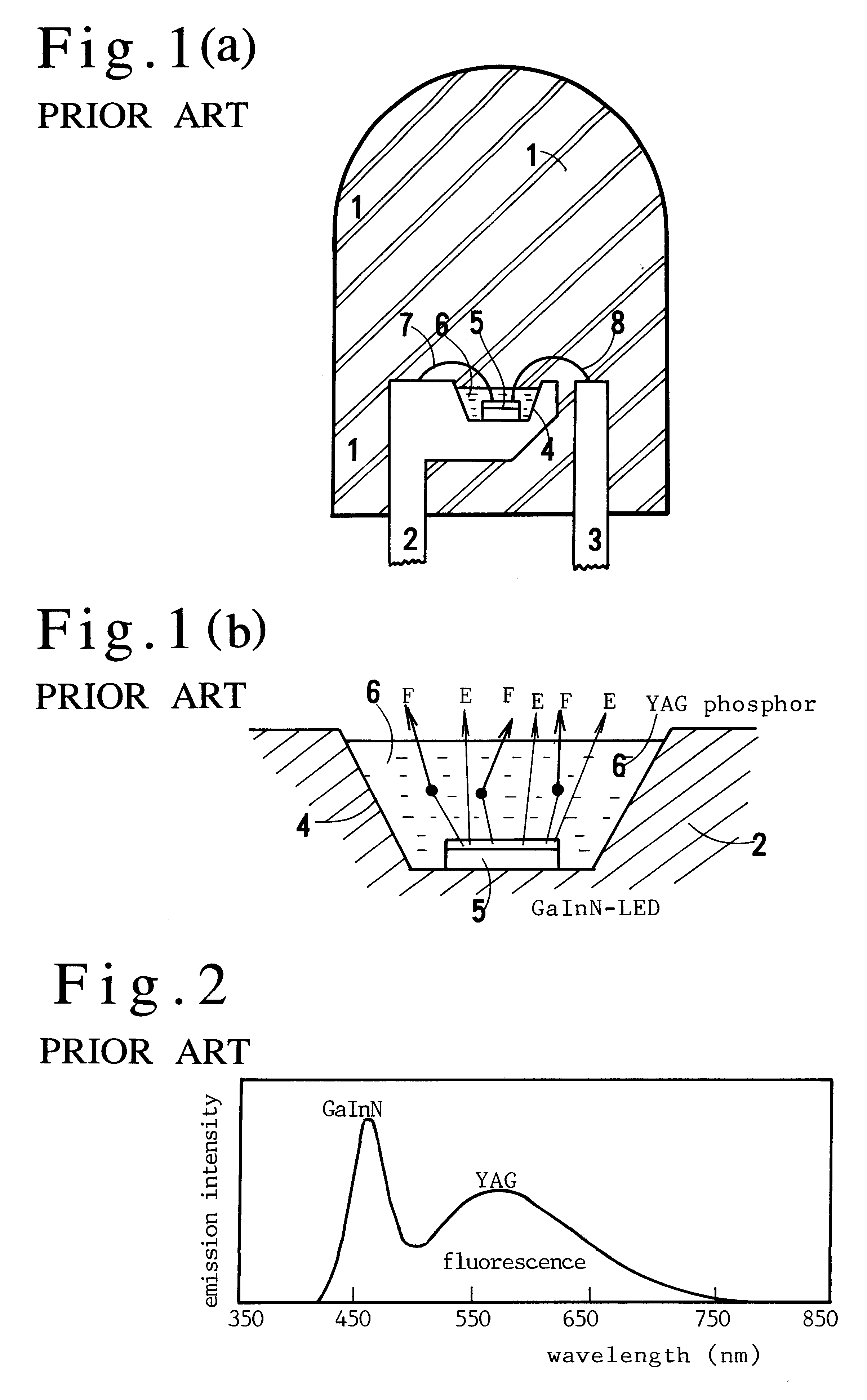
a technology of fluorescent led and substrate, which is applied in the direction of discharge tube/lamp details, discharge tube luminescnet screens, electric discharge lamps, etc., can solve the problems of short life of incandescent lamps, complicated led structure, and enhancing production costs

Inactive Publication Date: 2003-01-21
SUMITOMO ELECTRIC IND LTD
View PDF8 Cites 200 Cited by
  • Summary
  • Abstract
  • Description
  • Claims
  • Application Information

AI Technical Summary

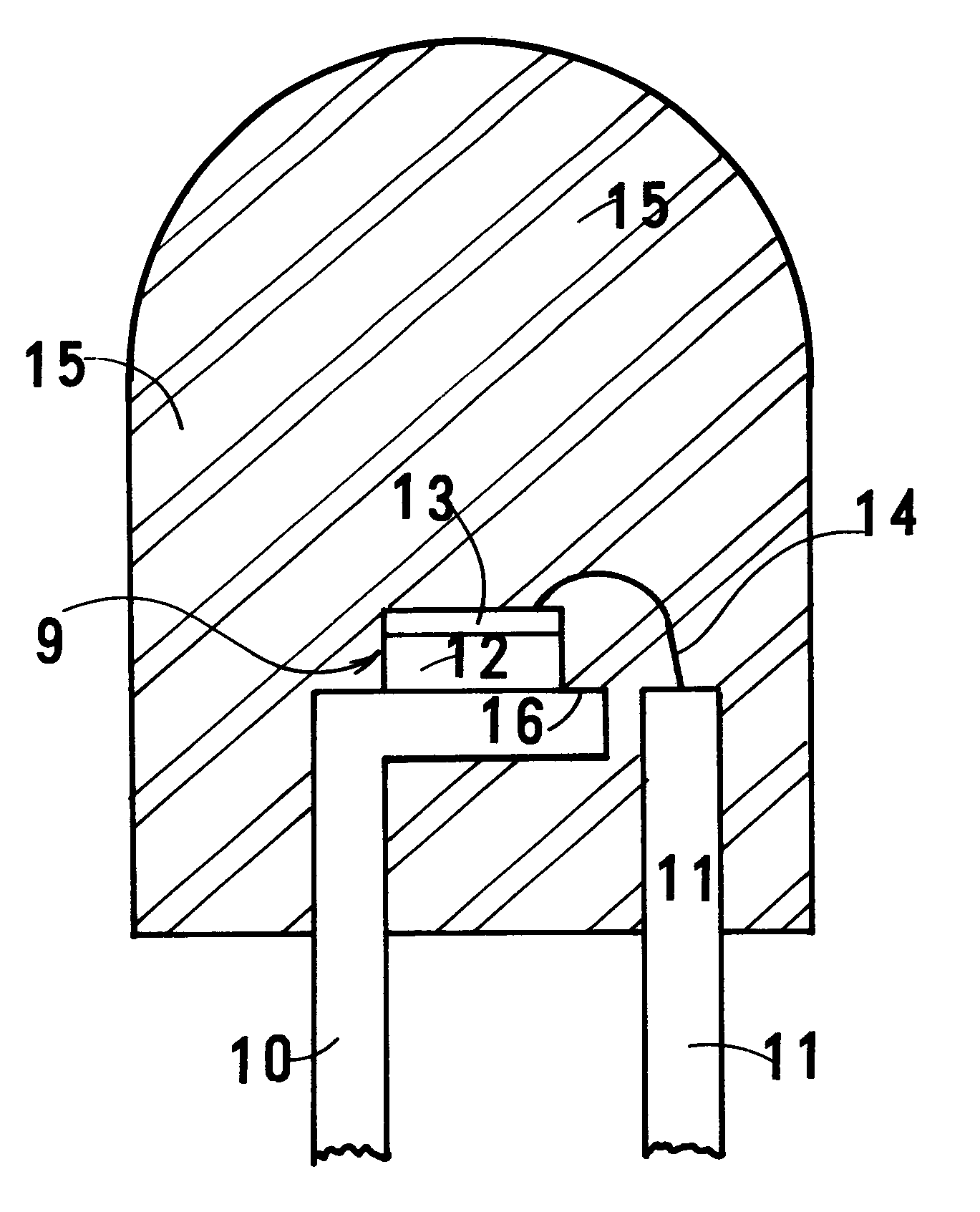
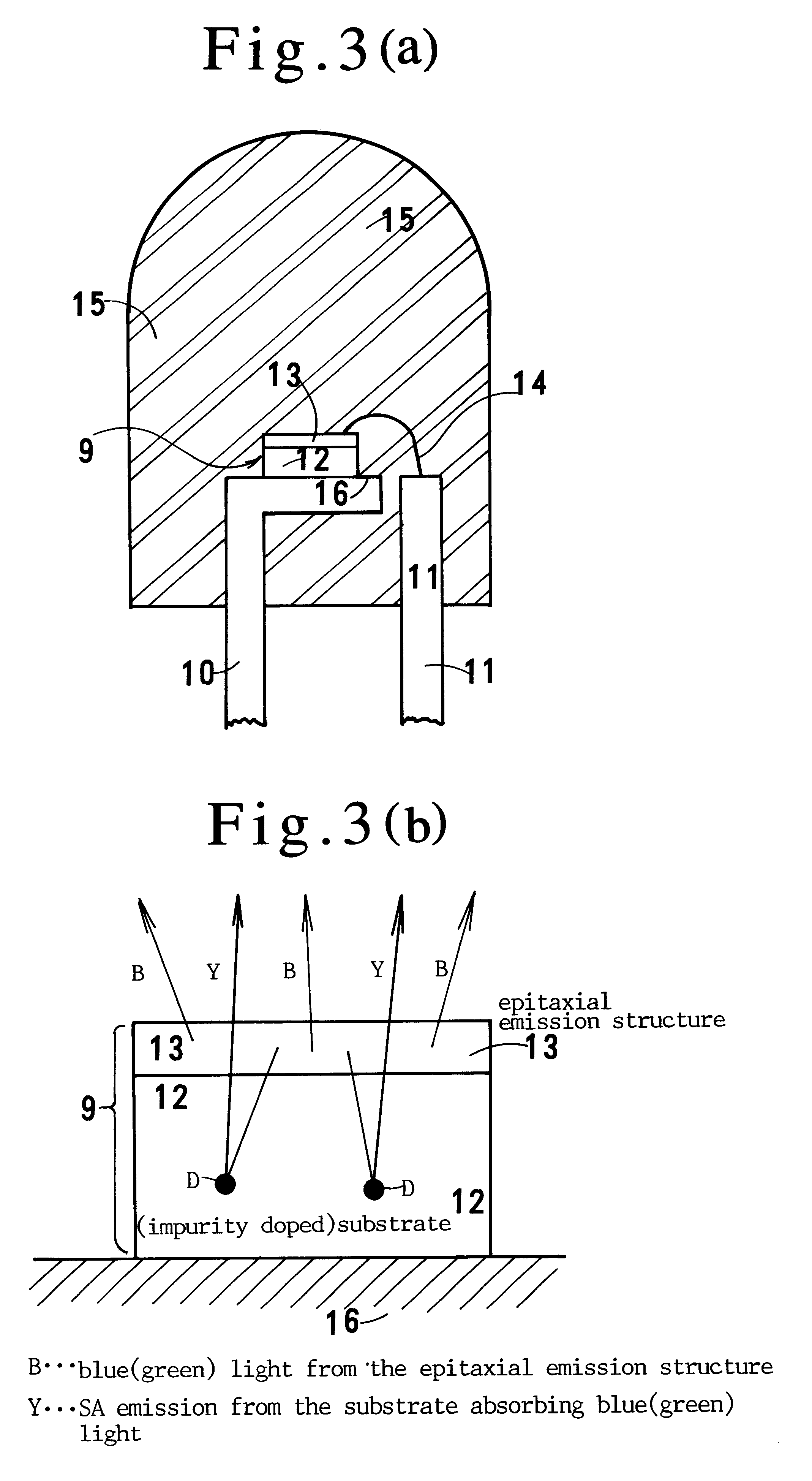
Problems solved by technology

However, an assembly of more than three different LEDs will complicate the LED structure and enhance the cost of the production.
However, incandescent lamps have a drawback of a short lifetime.
Incandescent lamps are plagued with low lightening efficiency.
Having a longer lifetime, fluorescent lamps are suffering from bulky, long and heavy apparatuses.
However, the applications of LEDs to displays are still restricted, since white, redpurple and pink cannot be produced by current LEDs.
Some drawbacks, however, accompany the proposed GaInN-YAG LED.
One drawback is extra existence of the YAG phosphor which is an entirely different material from the GaInN-LED.
The extra YAG raises the material cost and the production cost.
Another weak point is the low efficiency.
The YAG GaInN LED which is produced by covering the blue LED with the YAG has poor luminosity of 0.5 Cd and low external quantum efficiency of 3.5%.
Besides the poor transparency, YAG is suffering from low efficiency of converting blue light to yellow light.
The large thickness of the YAG increases the absorption of blue light in the YAG, which lowers both the luminosity and the efficiency.
However, the orange LEDs and the yellow LEDs are still suffering from low luminosity and high cost.
In order to compensate the poor expansion of injected electric current in the p-AlGaInP layer, the yellow LED should increase the thickness of the p-AlGaInP layer, which raises the production cost of MOCVD growth.
Further, the AlGaInP yellow LED is plagued with low luminosity.
The assembly of two LEDs has drawbacks o...

Method used


Image

  • Substrate-fluorescent LED
  • Substrate-fluorescent LED
  • Substrate-fluorescent LED

Examples


embodiment 1 ((

[Embodiment 1 ((I+Cu)ZnSe substrate, 630 nm; ZnSe / ZnCdSe active layer, 480 nm; pink, redpurple)]

A ZnSe substrate 20 doped with iodine (I) and copper (Cu) is prepared. An epitaxial emission structure having a ZnSe / ZnCdSe multiquantum well active layer 23 is built upon the ZnSe substrate as shown in FIG. 5.

The band tailing phenomenon allows the I+Cu doped ZnSe substrate 20 to absorb the light of a wavelength shorter than 510 nm (wavelength A=510 nm) and to produce the fluorescence (SA-emission) having a broad peak at 630 nm (wavelength B=630 nm) by the fluorescence centers (SA-centers) I and Cu. The band tailing phenomenon plays an important role in the present invention. A pure semiconductor of a band gap Eg is inherently transparent to the light of a wavelength .lambda. longer than the band gap wavelength .lambda.g (=hc / Eg) but opaque to the light of a wavelength .lambda. shorter than .lambda.g. Doping some impurities produces impurity levels near the valence band or the conduction ...

embodiment 2 ((

[Embodiment 2 ((Al+I)ZnSe substrate, 600 nm; ZnSe active layer, 465 nm; pink, redpurple)]

A ZnSe substrate 30 doped with iodine (I) and aluminum (Al) is prepared. An epitaxial emission structure having a ZnSe active layer 33 is built upon the ZnSe substrate 30 as shown in FIG. 8.

The band tailing phenomenon allows the I+Al doped ZnSe substrate 30 to absorb the light of a wavelength shorter than 510 nm (wavelength A=510 nm) and to produce the fluorescence(SA-emission) having a broad peak at 600 nm (wavelength B=600 nm) by the self-activated (SA) centers I and Al. Embodiment 2 allows the substrate to absorb the light of a wavelength till 510 nm (A) far longer than 465 nm (C=.lambda.g).

A less doped ZnSe substrate (.gamma.) of 1.times.10.sup.17 cm.sup.n-3 and a more doped ZnSe substrate (.delta.) of 5.times.10.sup.18 cm.sup.31 3 are prepared for investigating the influence of the difference of the dopant concentration upon the colors. Both substrates have the same thickness of 250 .mu.m. ...

embodiment 3 ((

[Embodiment 3 ((Si)AIGaAs substrate, 690 nm; ZnSSe / ZnCdSe, 520 nm & 550 nm; orange, yellow)]

A Si-doped n-AlGaAs layer 47 made on an Si-doped n-GaAs substrate 46 by a liquid phase epitaxy (LPE) is prepared as a substrate 40. An epitaxial emission structure having a ZnSSe / ZnCdSe active layer 43 is built upon the AlGaAs substrate 40 as shown in FIG. 11.

The band gap of the Al.sub.x Ga.sub.1-x As substrate can be changed within a scope from 570 nm to 860 nm by varying the Al ratio x. The substrate of embodiment 3 is an Al.sub.0.50 Ga.sub.0.50 As (x=0.50) crystal doped with Si on the GaAs base 46. The Si doped AlGaAs substrate 40 allows to absorb the light of a wavelength shorter than 640 nm (wavelength A=640 nm) and to produce the photo-luminescence having a broad peak at 690 nm (wavelength B=690 nm) by the recombination center Si.

The epitaxial emission structures of peak wavelengths (C) 520 nm (.epsilon.) and 550 nm (.zeta.) are fabricated upon the AlGaAs substrate 40 by an MBE method, ...


PUM


Abstract

A substrate-fluorescent LED having a fluorescent-impurity doped substrate and an epitaxial emission structure including an active layer and being made on the substrate. The epitaxial emission structure emits blue or green light corresponding to the band gap of the active layer. The substrate absorbs a part of the blue or green light and makes fluorescence of a longer wavelength. Neutral color light or white light is emitted from the LED. The fluorescent substrate is n-AlGaAs(Si dope), GaP(Zn+O dope), ZnSe(Cu+I, Ag+I, Al+I dope), GaN(O.C.Va(N) dope) or so.

Description

1. Field of the InventionThis invention relates to a new LED which emits complex light with a spectrum having two peaks, in particular, relates to a single LED having a substrate and an active layer which produces neutral colors, e.g., pink, redpurple, orange, yellow or white color by synthesizing the band gap emission from the active layer and the fluorescence from the substrate.This application claims the priority of Japanese Patent Applications No. 10-212381 (212381 / 1998) filed on Jul. 28, 1998 and No. 10-323401 (323401 / 1998) filed on Nov. 13, 1998, which are incorporated herein by reference.2. Description of Prior ArtThere are already various high luminous LEDs for emitting various monochromatic colors on sale. The LEDs having an active layer of AlGaAs or GaAsP are prevalent as red color LEDs. Red color LEDs emitting red light more than several candelas (Cd) are produced at a low cost. The LEDs emitting the colors other than red are also prevailing. Green-yellowgreen LEDs are pr...

Claims


Application Information

Patent Timeline
IPC IPC(8): H01L33/00H01L33/50
CPCH01L33/08H01L2224/48091H01L2224/48247H01L2224/48257H01L2924/00014
Inventor MATSUBARA, HIDEKITAKEBE, TOSHIHIKOMOTOKI, KENSAKU
Owner SUMITOMO ELECTRIC IND LTD
Why Eureka
Try Eureka