Nanotube-based electron emission device and systems using the same

a technology of electron emission device and nanotube, which is applied in the direction of material analysis using wave/particle radiation, instruments, heat measurement, etc., can solve the problems of complex operation of cfe in a stable manner, the angular divergence of beams is minimal, and the tendency of ions to accelerate towards the emitter is significantly decreased

Inactive Publication Date: 2003-01-28
EL MUL TECH
View PDF16 Cites 51 Cited by
  • Summary
  • Abstract
  • Description
  • Claims
  • Application Information

AI Technical Summary

Benefits of technology

A central idea of the present invention is based on the implementation of an electron source with a cathode-electrode which is formed by one or more nanotubes within a specially designed environment, and is associated with one or more gates formed by an anode electrode. According to the technique of the present invention, this is done in a way that minimizes the angular divergence of the beam to the extent that the invention discloses a gun that produces a nearly laminar electron beam. This electron source allows a significant fraction of the current that is emitted from the gun, to be used in a probe. Such an electron source may be used in an electron microscope, either for scanning or transmission purposes, in a lithography tool, in a field emission display and for direct writing purposes.
The nanotube-based electron gun is expected to require lower vacuum conditions (about 10.sup.-6 -10.sup.-7 Torr), as compared to that required by conventional electron sources. The relaxed vacuum requirement is due to the fact that nanotubes are less sensitive to adsorption than conventional emitters. Another reason for the lower vacuum requirement is the "point on a plane" configuration: the nanotubes are situated on a conducting surface, the lines of the electric field are effectively directed between the two planes. Thus, the tendency of ions to be accelerated towards the emitter is significantly decreased.
According to the gun design proposed in the invention, the nanotubes can be assembled in a way that provides very high brightness. The high brightness, combined with the low energy spread (about 0.1 eV), enables a resolution of less than 1 nm to be provided with relatively low accelerating voltages. Since the brightness of the beam, as it exits the electron gun, is high, an optical column attached to the gun can be significantly shorter than the micro-columns known so far. Since heating of the tip-electrode to high temperatures is not required and s

Problems solved by technology

Moreover, CFE suffer from ultra-high vacuum requirements (e.g., 10.sup.-9 -10.sup.-10 Torr), which is a major factor in the cost of a CFE-based device.
Due to the unavoidable adsorption of molecules on the tip-like cathode-electrode, it is complicated to operate CFE in a stable manner.
A further drawback is associated with the need to stabilize the system at a high working temperature, i.e., about 1800.degree. C.
This may damage the sample and/or cause undesirable charging thereof To solve this problem, beam deceleration may be employed.
However, this complicates the construction of an electron beam column, and enhances chromatic aberrations.
As a result of the above disadvantages of the conventional electron sources, their use in EM and EBL tools make these tools expensive and bulky.
This impedes their application as integrated tools.
This slows the production.
Moreover, any unnecessary handling of such delicate workpieces as semiconductor wafers is undesirable.
As for the lithography tools, it is a core challenge of the semiconductor industry, to go beyond optical resolution, which currently limits the minimal feature size of the active elements of a semiconductor device.
Although these technologies have been known for several years, none of them is used in commercial applications.
This is due to the following reasons: the miniaturized arrayed operation is limited by the absence of an adequate electron source, which has the desired electron optical quality (high brightness and low energy spread), which is compatible with miniaturization and with silicon technologies,

Method used


Image

  • Nanotube-based electron emission device and systems using the same
  • Nanotube-based electron emission device and systems using the same
  • Nanotube-based electron emission device and systems using the same

Examples


Embodiment Construction

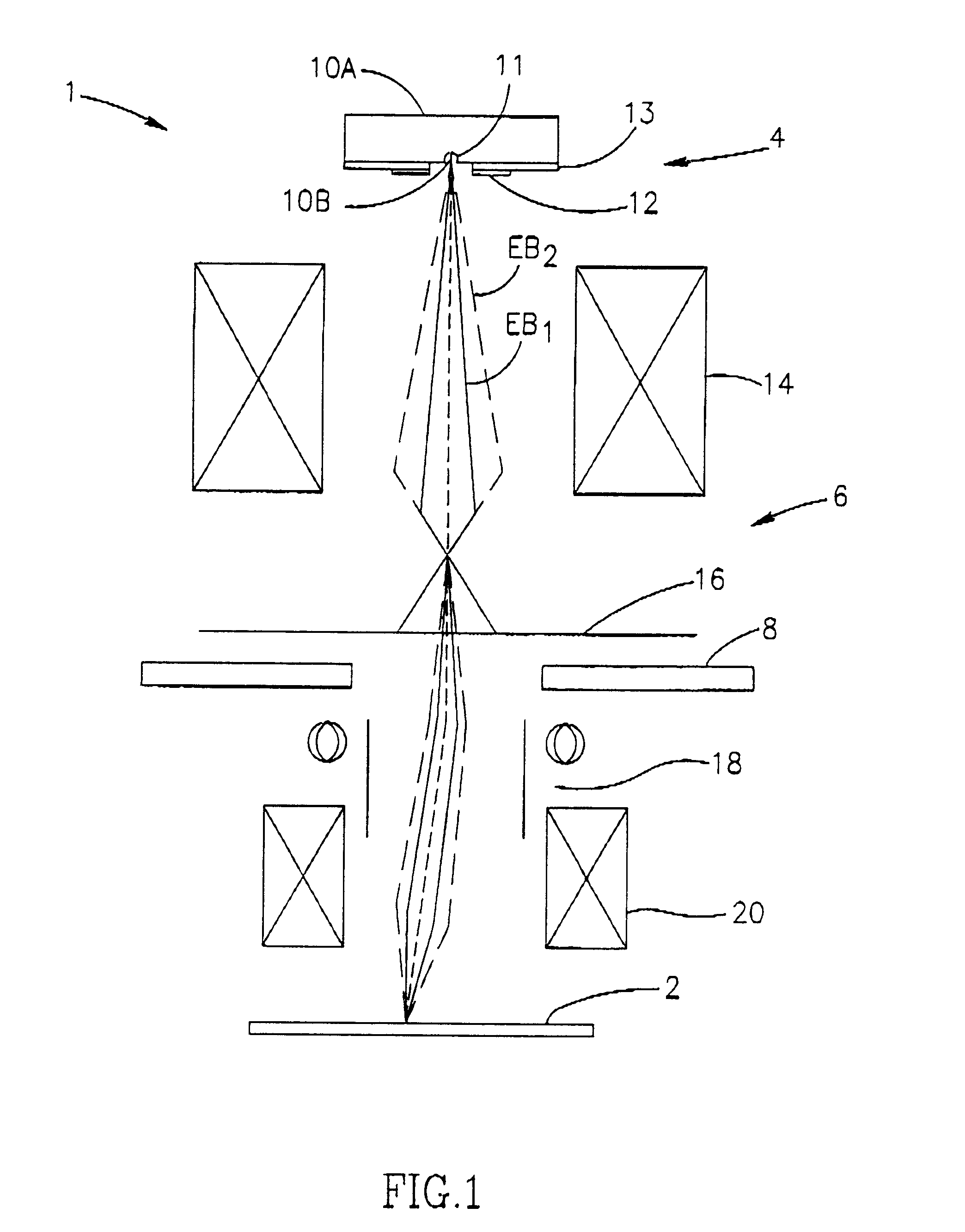
Referring to FIG. 1, there is schematically illustrated a scanning electron microscope, generally designated 1, constructed according to one embodiment of the invention, for inspecting a sample 2 or for processing it with an electron beam. The microscope 1 comprises such main constructional parts as an electron source device 4 and an electron beam column 6 that directs a primary beam towards the sample 2 and directs secondary and back-scattered electrons towards a detector means 8. The latter is appropriately accommodated in the path of electrons knocked out from the sample 2 as a result of its interaction with a primary electron beam.

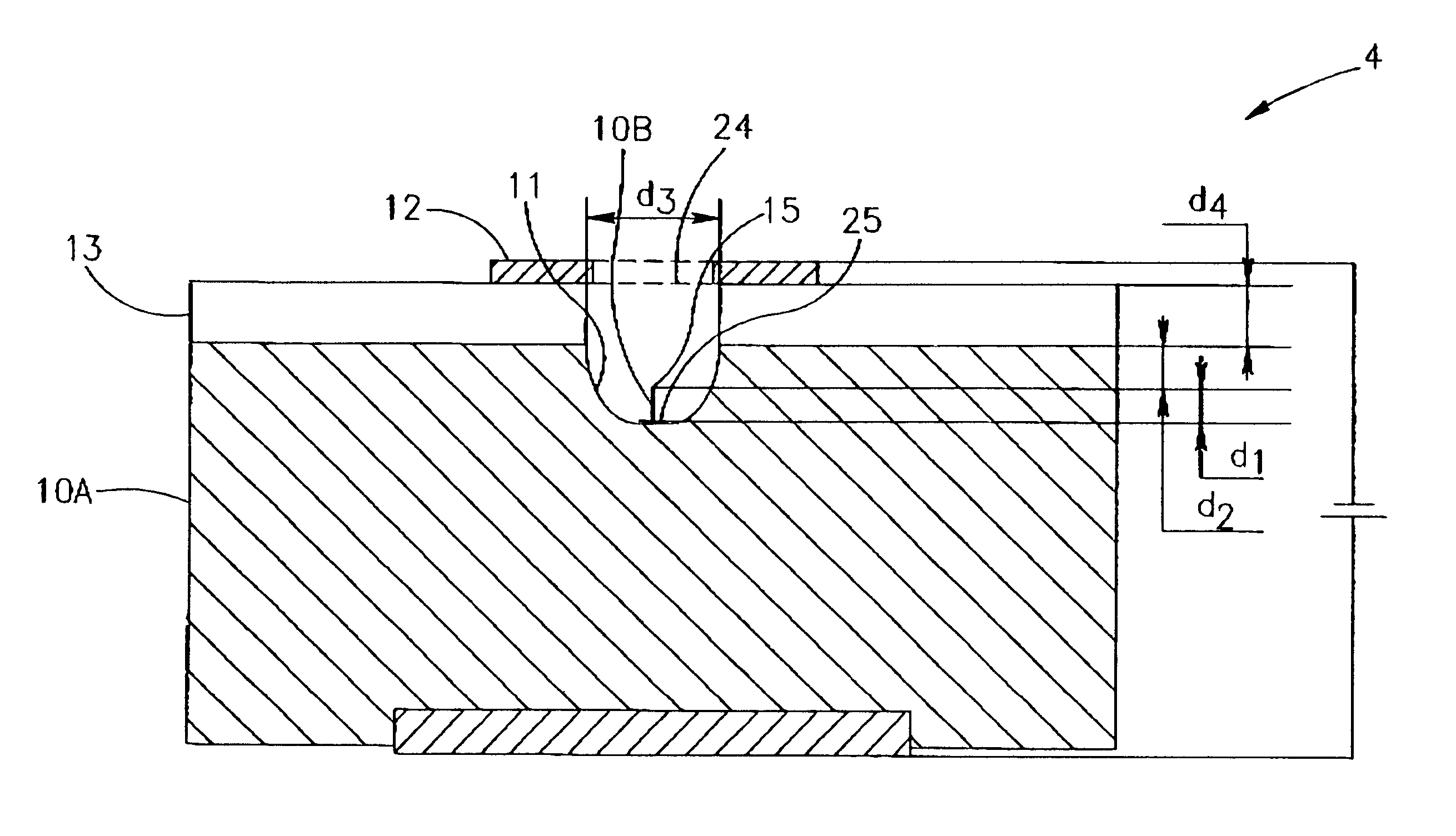
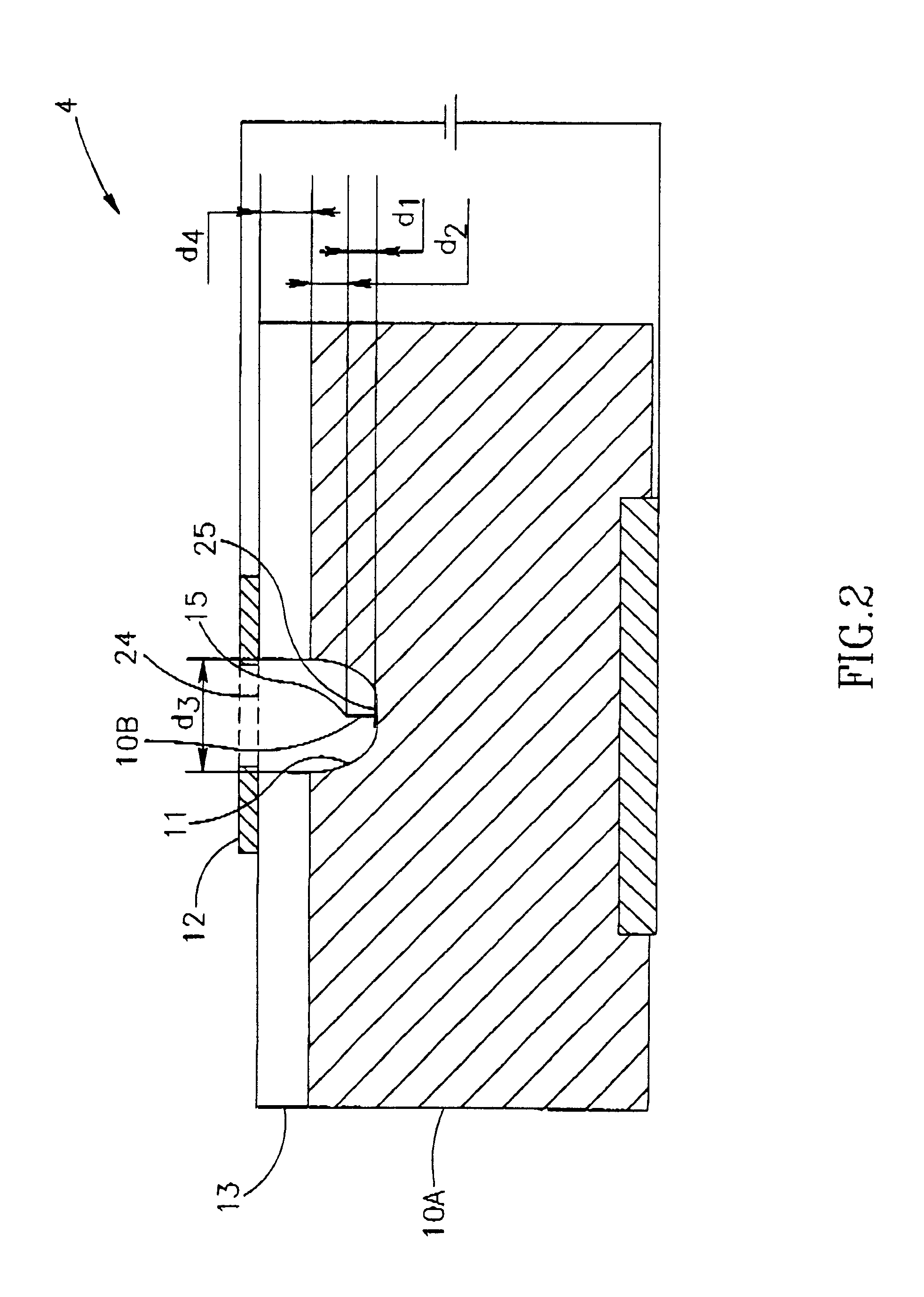
As more specifically illustrated in FIG. 2, the electron source device 4 according to the present invention comprises a single nanotube or nanotube bundle 10B located in a crater 11 formed in a conducting layer 10A, and an anode-electrode 12. A nanotube 10B is formed on a metal catalyst 25 on the bottom of the crater 11, such that a tip 15 of the nanot...


PUM


Abstract

A device that produces an electron beam with high optical quality for processing a sample, is presented. The optical quality is manifested by very high brightness and low energy spread. The device includes an electron source device comprising an electrode in the form of a shaped first layer, preferably in the form of a conducting crater carrying at least one nanotube, and an extracting electrode, which is formed with at least one aperture and is insulated from the firs layer. The source can be used in any column that requires such properties. The column according to the invention may be a full size or a miniature electron microscope, a lithography tool, a tool used for direct writing of wafers or a field emission display.

Description

This invention is generally in the field of electron emission based techniques, such as electron microscopy (EM), specifically scanning electron microscopy (SEM), and electron beam lithography (EBL), utilizing a nanotube-based electron emission device, with high electron optical quality, specifically high brightness and low energy spread. The electron emission device of the present invention can be used with any electron beam column or other system that requires such properties.It is the common goal of various applications utilizing an electron beam source, such as SEM and EBL, to have a simple and stable electron beam source, in particular, a source capable of being installed in a miniature device and having high electron optical quality. The simplicity of the electron source is defined by its working conditions, such as operating vacuum and temperature parameters. As for the optical quality, it is predominantly determined by the brightness (i.e., current density per solid angle) a...

Claims


Application Information

Patent Timeline
IPC IPC(8): G01N23/02G01N23/04B82B3/00H01J1/304H01J29/04H01J37/06H01J37/073H01J37/28H01J37/305H01L21/027
CPCB82Y10/00G01N23/04Y10S977/939G01N23/2251
Inventor EITAN, GUYZIK, ORYROSENBLATT, DAVID
Owner EL MUL TECH
Why Eureka
Try Eureka