Group III nitride light emitting devices with gallium-free layers

Inactive Publication Date: 2003-03-18
CREE INC
View PDF31 Cites 48 Cited by
  • Summary
  • Abstract
  • Description
  • Claims
  • Application Information

AI Technical Summary

Benefits of technology

Therefore, it is an object of the present invention to produce light emitting diodes and laser

Problems solved by technology

Despite widespread use, LEDs are somewhat functionally constrained, be cause the color that a given LED can produce is limited by the nature of the semiconductor material used to fabricate the LED.
More common semiconductor materials such as silicon, gallium phosphide, or gallium arsenide are unsuitable for producing blue light because their bandgaps are approximately 2.26 eV or less, and in the case of silicon, are indirect semiconductors and inefficient light emitters.
The necessity of a third particle, the phonon, makes indirect radiative transitions less likely, thereby reducing the light emitting efficiency of the device.
Although Group III nitrides offer a direct transition over a wide bandgap energy range, the material presents a particular set of technical manufacturing problems.
In particular, no commercially-viable technique has yet emerged for producing bulk single crystals of gallium nitride (GaN) that are capable of functioning as appropriate substrates for the gallium nitride epitaxial layers on which photonic devices would be formed.
Using different substrates, how

Method used


Image

  • Group III nitride light emitting devices with gallium-free layers
  • Group III nitride light emitting devices with gallium-free layers
  • Group III nitride light emitting devices with gallium-free layers

Examples


example 1

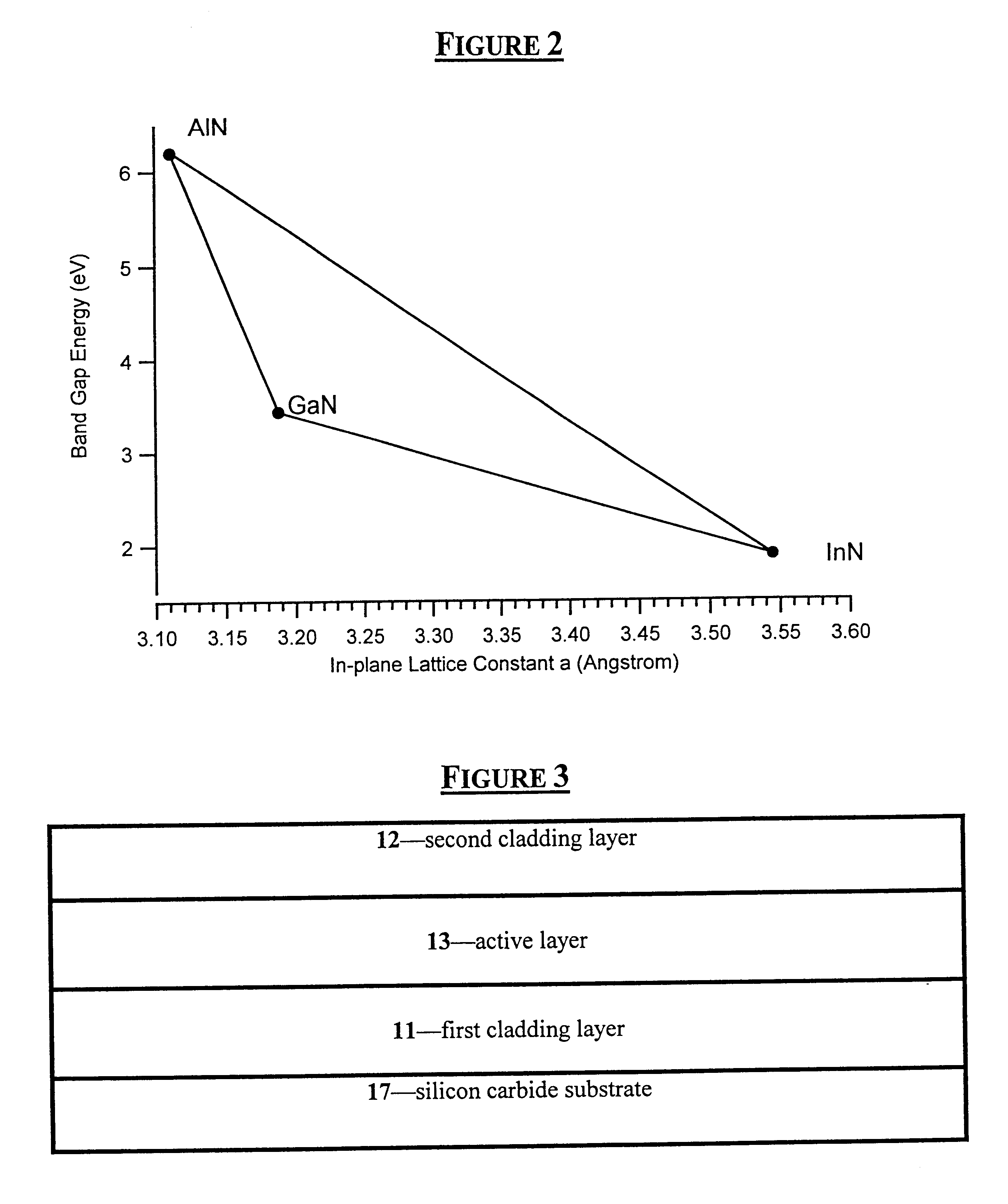
The cladding layers for a blue LED (425 nm<.lambda.<480 nm) must have a band-gap energy greater than that of the blue active layer (2.58-2.92 eV). For the ternary In.sub.x Al.sub.1-x N, the bandgap energy of the ideal crystal remains a matter of research and debate. This is primarily due to the difficulty in growing high quality, uniform epitaxial layers of the solid solution that are thick enough (approximately 0.2 .mu.m) for optical transmission measurements to determine the bandgap energy. From current data, In.sub.0.17 Al.sub.0.83 N has a bandgap energy of 2.9-3.0 eV. See S. Yamaguchi, M. Kariya, S. Nitta, T. Takeuchi, C. Wetzel, H. Amano, and I. Akasaki, Appl. Phys. Lett. 76 876 (2000). Therefore, cladding layers for blue LEDs should have an indium molar fraction of less than 0.17. See K. S. Kim, A. Saxler, P. Kung, M. Razeghi, and K. Y. Kim, Appl. Phys. Lett. 71 800 (1997).

example 2

Blue light emissions are produced for the ternary In.sub.x Al.sub.1-x N between 0.14

It will be understood by those of skill in the art that these are bulk emission values and that growth of the material as quantum wells will produce quantum confinement that will blue shift these emission wavelengths.

It will be further appreciated by those of ordinary skill in the art that, as used herein, the concept of one layer being "between" two other layers does not necessarily imply that the three layers are conti...


PUM


Abstract

The present invention is a semiconductor structure for light emitting devices that can emit in the red to ultraviolet portion of the electromagnetic spectrum. The semiconductor structure includes a first cladding layer of a Group III nitride, a second cladding layer of a Group III nitride, and an active layer of a Group III nitride that is positioned between the first and second cladding layers, and whose bandgap is smaller than the respective bandgaps of the first and second cladding layers. The semiconductor structure is characterized by the absence of gallium in one or more of these structural layers.

Description

The present invention relates to semiconductor structures of light emitting devices, particularly light emitting diodes and laser diodes formed from Group III nitrides, which are capable of emitting light in the red to ultraviolet portions of the electromagnetic spectrum.Photonic semiconductor devices fall into three categories: devices that convert electrical energy into optical radiation (e.g, light emitting diodes and laser diodes); devices that detect optical signals (e.g., photodetectors); and devices that convert optical radiation into electrical energy (e.g., photovoltaic devices and solar cells). Although all three kinds of devices have useful applications, the light emitting diode may be the most commonly recognized because of its application to various consumer products and applications.Light emitting devices (e.g., light emitting diodes and laser diodes), herein referred to as LEDs, are photonic, p-n junction semiconductor devices that convert electrical power into emitte...

Claims


Application Information

Patent Timeline
IPC IPC(8): H01L33/00H01L33/32H01S5/323H01S5/343
CPCH01L33/32H01L33/007
Inventor EDMOND, JOHN ADAMDOVERSPIKE, KATHLEEN MARIEKONG, HUA-SHUANGBERGMANN, MICHAEL JOHN
Owner CREE INC
Why Eureka
Try Eureka