

Manufacturing method of a multilayered printed circuit board having an opening made by a laser, and using electroless and electrolytic plating
a printed circuit board and laser cutting technology, applied in the direction of manufacturing tools, printed element electric connection formation, etching metal masks, etc., can solve the problems of unsatisfactory connection reliability, inability to form a conductive circuit with fine pitch, and inability to reduce the width of the conductive circui
- Summary
- Abstract
- Description
- Claims
- Application Information
AI Technical Summary
Benefits of technology
Problems solved by technology
Method used
Image

Examples
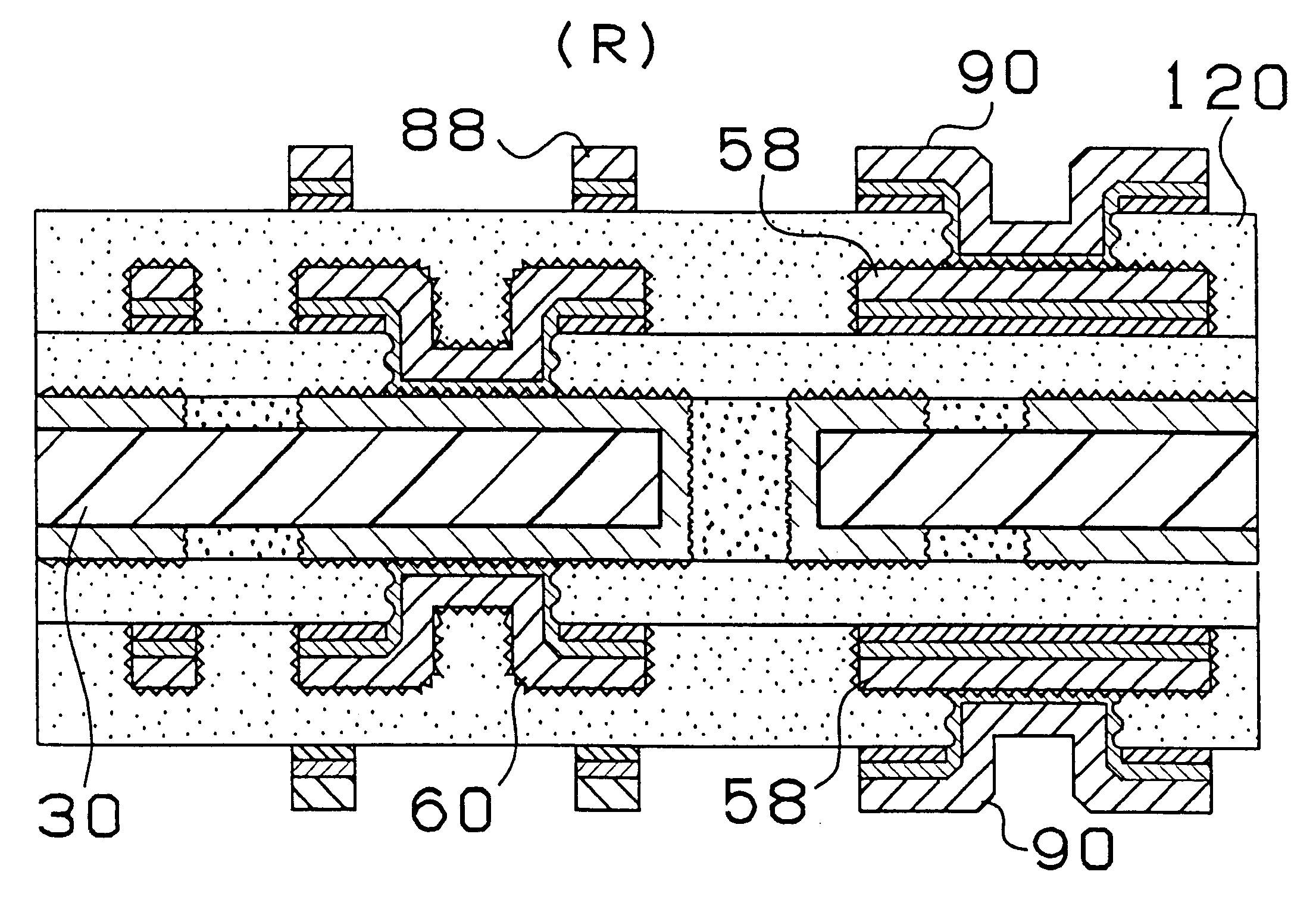
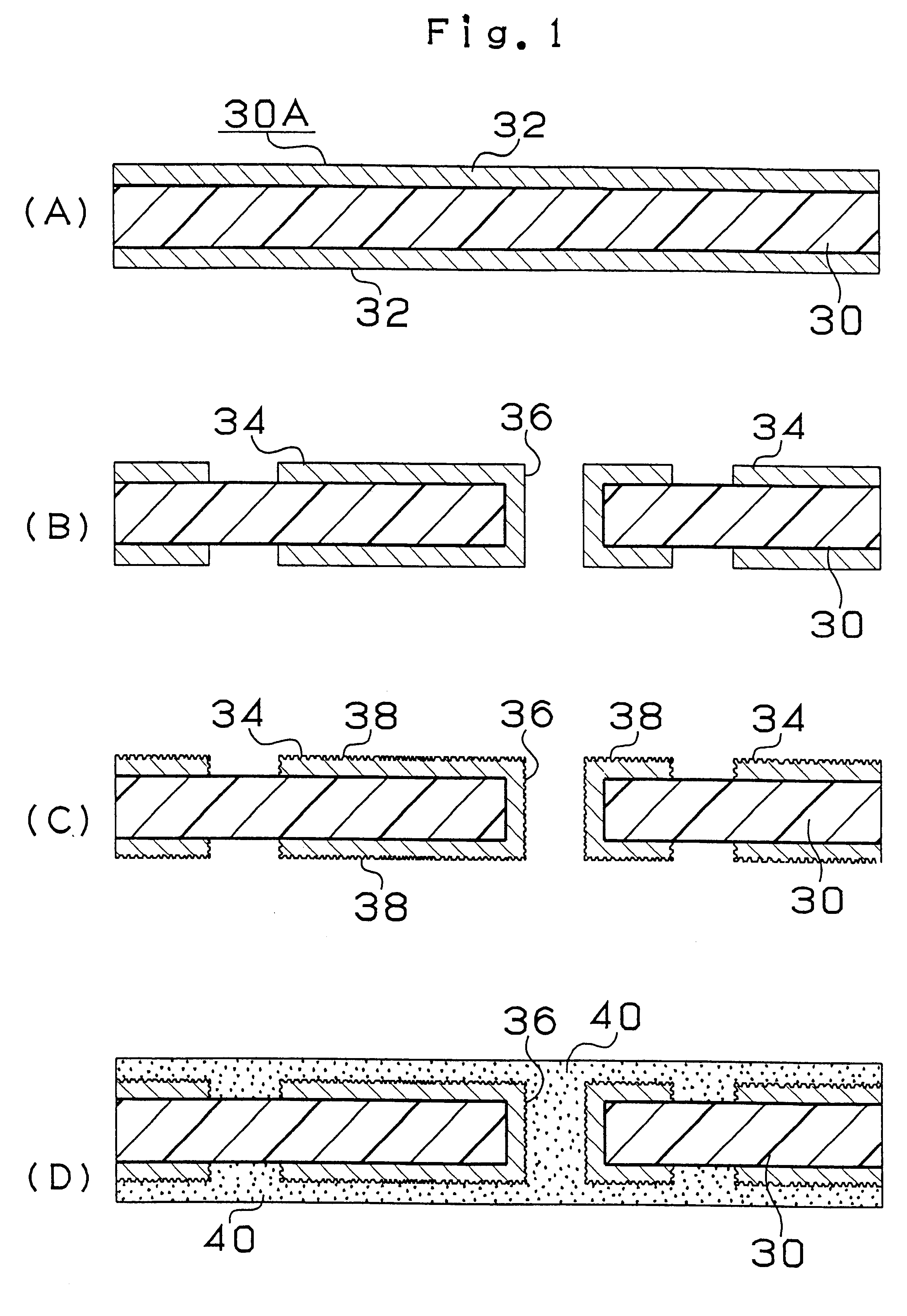
first embodiment
The first embodiment is able to form the opening 20a with the small-output laser or such that the number of operations for applying the pulse laser beams is reduced. Therefore, occurrence of undercut in the resin 20 for forming interlayer insulating resin layer can be prevented (see FIG. 3(L)). Therefore, the reliability of the connection of the via hole can be improved. It is preferable that the thickness of the metal film is reduced to 5 .mu.m to 0.5 .mu.m by etching. If the thickness of the metal film is larger than 5 .mu.m, undercut occurs. If the thickness is not larger than 0.5 .mu.m, the function of the conformal mask cannot be realized.
When the interlayer insulating resin layer forming resin having the metal film formed thereon is pressed against the substrate on which the conductive circuit will now be formed and then etching is performed, the thick metal film exists as a reinforcing member until the pressing operation is performed. Therefore, an excellent handling characte...
second embodiment
A multilayered printed circuit board and a manufacturing method therefor according to a second embodiment of the present invention will now be described.
As the substrate for use in the second embodiment may be a resin substrate, such as a glass-cloth epoxy resin substrate, a glass-cloth bis maleimide-triazine resin, glass-cloth fluorine resin substrate; a copper-plated laminated board obtained by bonding copper foil to the foregoing resin substrate, a metal substrate or a ceramic substrate.
A conductive circuit is provided for the upper surface of the substrate. The conductive circuit can be formed by electroless plating or electrolytic plating. When the copper-plated laminated board is employed, the conductive circuit can be formed by an etching process.
Then, an insulating resin layer is formed. In the second embodiment, the insulating resin layer is irradiated with a laser beam so that an opening for forming the via hole is formed. Therefore, the foregoing insulating resin layer is...
third embodiment
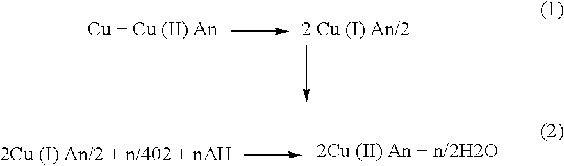
A multilayered printed circuit board and a manufacturing method therefor according to a third embodiment of the present invention will now be described. The method of manufacturing the multilayered printed circuit board according to the third embodiment has the steps of (1) forming a conductive circuit; (2) forming an interlayer insulating resin layer on the conductive circuit; (3) applying a laser beam to form an opening for forming a via hole in the interlayer insulating resin layer; and (4) forming another conductive circuit having a via hole on the interlayer insulating resin layer, wherein a solution containing cupric complex and organic acid is used to coarsen the surface of the conductive circuit before the process (2).
The multilayered printed circuit board obtained by the foregoing manufacturing method incorporates the conductive circuit, the surface of which is coarsened by the etching solution containing the cupric complex and the organic acid. Moreover, the interlayer ins...
PUM
| Property | Measurement | Unit |
|---|---|---|
| thickness | aaaaa | aaaaa |
| thickness | aaaaa | aaaaa |
| diameter | aaaaa | aaaaa |
Abstract
Description
Claims
Application Information