Semiconductor storage device
a technology of semiconductor devices and storage devices, applied in semiconductor devices, semiconductor/solid-state device details, capacitors, etc., can solve problems such as the deformation of capacitor characteristics or the peeling of electrodes
- Summary
- Abstract
- Description
- Claims
- Application Information
AI Technical Summary
Benefits of technology
Problems solved by technology
Method used
Image
Examples
embodiment 1
(Embodiment 1)
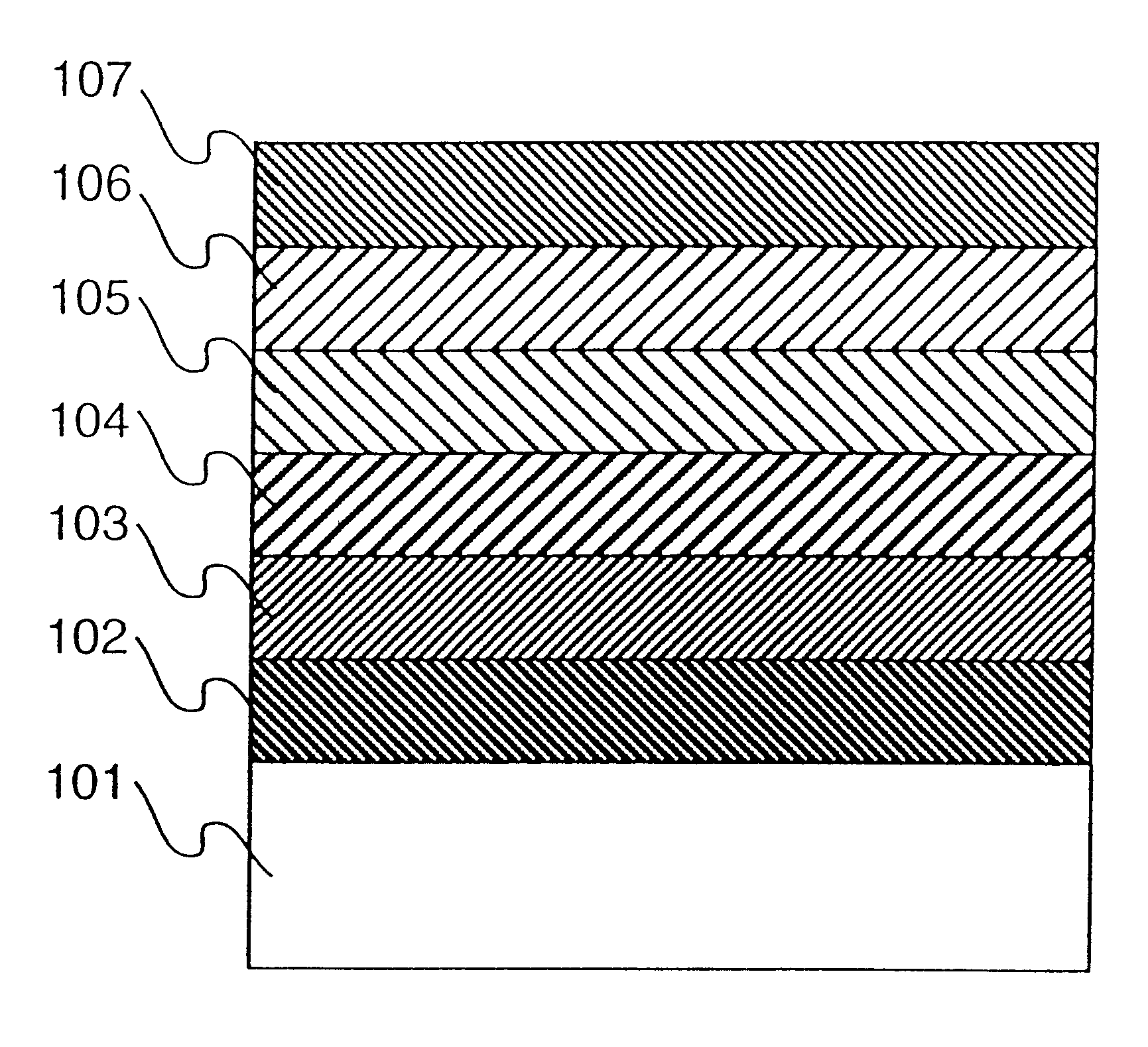
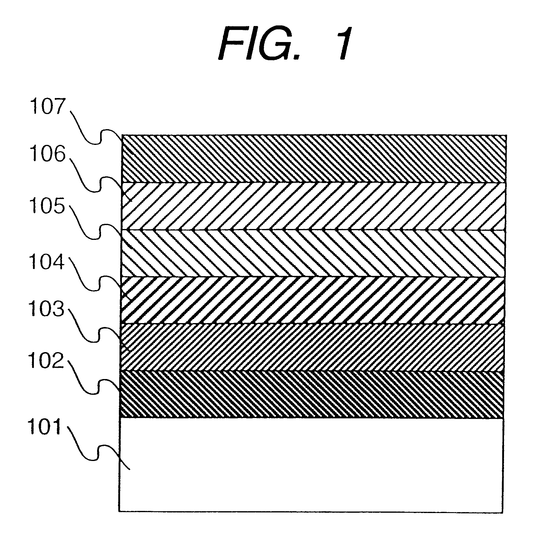
A preferred embodiment of the invention will be described hereinbelow with reference to FIG. 1.
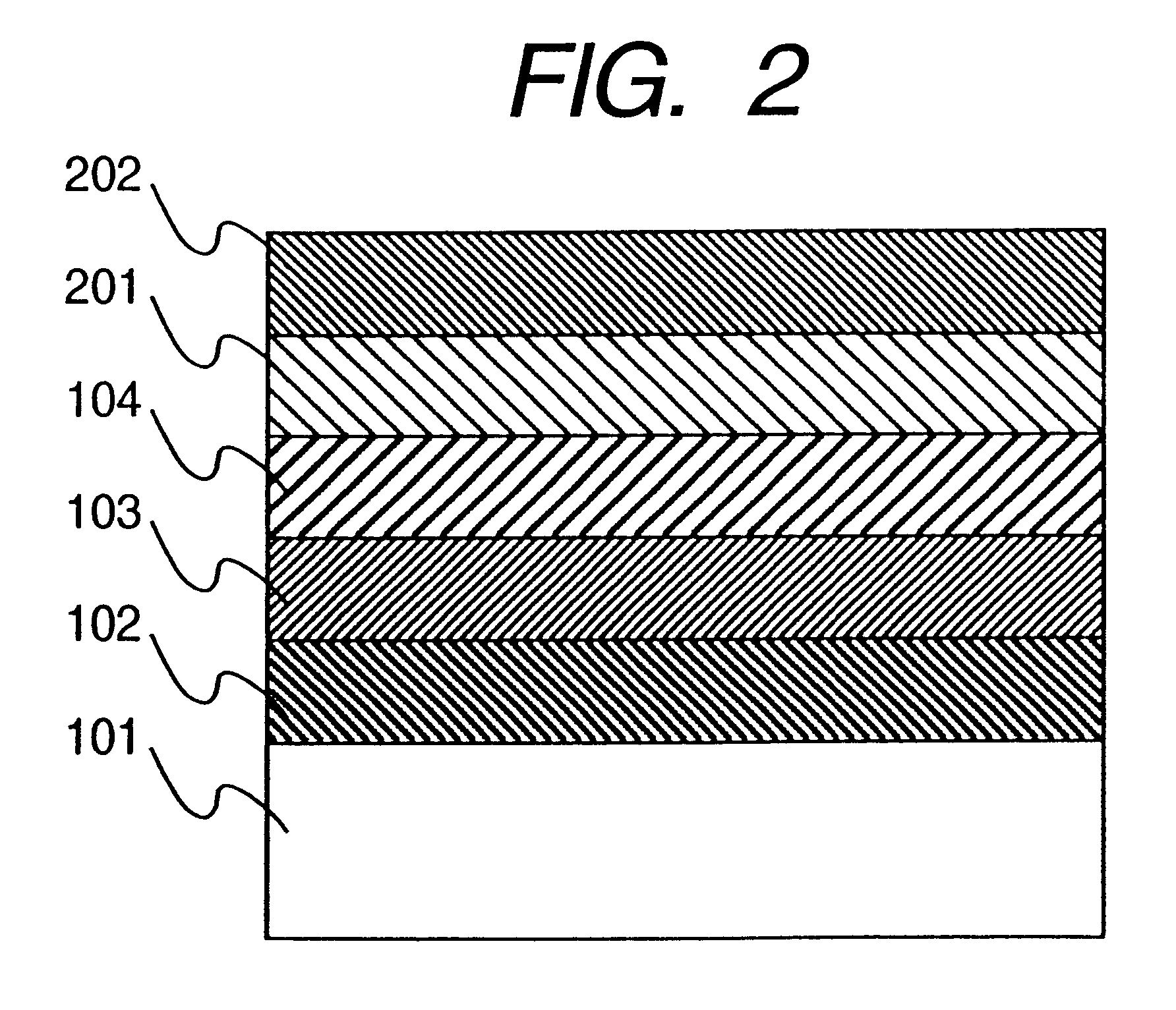
In a capacitor of the invention, a lower electrode (102) and a high dielectric constant or ferroelectric thin film (103) are formed by a known method on either a device layer or a semiconductor area (101) constructing a transistor, which is formed by a known method. On the film (103), an upper layered electrode consisting of four layers of the invention is formed. That is, the upper layered electrode consists of a Schottky barrier layer (104), a hydrogen diffusion preventing layer (105), a reaction preventing layer (106), and an adsorption inhibiting layer (107).
Although the upper layered electrode is comprised of four layers in FIG. 1, the number of stacked layers is decreased by using a layer having functions of a plurality of layers or the function of one layer can be realized by a plurality of layers, so that the number of stacked layers may increase or decrease. All of t...
embodiment 2
(Embodiment 2)
A method of fabricating the layered upper electrode will now be described more specifically.
FIG. 3 shows a preferred embodiment of a capacitor according to the invention. On an active device layer (101) including a transistor formed by a known method, platinum (102) is deposited to 100 nm as a lower electrode by DC sputtering. Subsequently, PZT is deposited to 50 nm by radio frequency sputtering. After that, a heat treatment at 650.degree. C. is performed in oxygen, thereby forming the high dielectric constant or ferroelectric layer (103). 50 nm of platinum (301) is then formed as a Schottky barrier layer. Subsequently, 100 nm of tungsten (302) as a diffusion barrier layer, 50 nm of titanium nitride (303) as a reaction preventing layer, and 100 nm of silver (304) as an adsorption inhibiting layer are formed, thereby obtaining a layered upper electrode.
The electrical breakdown voltage distribution after the heat treatment in hydrogen of the capacitor having the structur...
embodiment 3
(Embodiment 3)
Another preferred embodiment of the invention will be described with reference to FIG. 6. On the active device layer (101) including a transistor formed by a known method, platinum (102) is deposited to 100 nm as a lower electrode by DC sputtering. Then, on the substrate heated to 500.degree. C., BST is deposited to 50 nm by the radio frequency sputtering. After that, a heat treatment at 650 .degree. C. is performed in oxygen, thereby forming a high dielectric layer (601). Subsequently, platinum (301) is deposited to 50 nm as a Schottky barrier layer. In the embodiment, ruthenium oxide (602) is deposited to 50 nm as a hydrogen diffusion preventing layer by reactive sputtering using oxygen. On the layer (602), a layered film (603) of 50 nm of metal ruthenium and 50 nm of titanium nitride is formed in this order as a reaction preventing layer by sputtering. On the layer (603), aluminum (604) is deposited to 100 nm as an adsorption inhibiting layer, thereby obtaining a la...
PUM
 Abstract
Description
Claims
Application Information


