Method and apparatus for simulating manufacturing, electrical and physical characteristics of a semiconductor device

a semiconductor device and simulation method technology, applied in the direction of instruments, analogue processes for specific applications, electric/magnetic computing, etc., can solve the problems of tighter design criteria, increased complexity of equipment used in semiconductor processing, and strong increase of the number of metal layers

Inactive Publication Date: 2004-11-30
KK TOSHIBA
View PDF9 Cites 52 Cited by
  • Summary
  • Abstract
  • Description
  • Claims
  • Application Information

AI Technical Summary

Problems solved by technology

Semiconductor design and fabrication have a wide variety of issues, relating to LSI fabrication, process design, system design, device design, and so on.
From FIG. 2, it is understood that the continual drive towards smaller feature size in device fabrication results in tighter design criteria and increased complexity of equipment used in semiconductor processing.
The increase of the integration density, while maintaining the same RC signal delay leads to a strong increase of the number of the metal layers.
However, the more aggressive the rules have been, the greater the probability of improvements in circuit performance.
This improvement has been at the expense of yield.
If the designer has not carefully considered this step in the overall design process, it is often impossible to test the circuit and determine whether or not the specifications have been met.
So, it is now very difficult to estimate realistically the value of resistance.
Other design phase difficulties exist.
The switching speed of CMOS gates is limited by the time taken to charge and discharge the load capacitance C.sub.L.
For the most part, this has not been the approach of the part due to the predominant influence of transistors on the key theoretical and practical limits on microchips.
In other words, designing of wiring layout and wiring materials becomes an important issue more than transistor designing.
Here, it is easily understood that it would be very difficult to estimate overlap capacitance or peripheral capacitance and the like.
So, a precise estimation of delay time or system design is not obtained in the model.
The phase from TEG (test element group) test fabrication to check the system performance is still very much time-consuming.
Because, in the product LSI, electric characteristics of each device cannot be measured directly.
Moreover, conventional TCAD now faces a huge barrier not previously experienced.
The problems facing the development of GSI are that because the simulations use a simple equivalent circuit method, it is difficult to precisely estimate delay time, performance, and the like.
Because there is a lack of synthesis analysis across the entire lumped element devices, such criteria apply only to the interconnect process.
By not incorporating cross talking in the scaled device, the full development of scaled device design is still impeded.
However, basically, such improvements do not make direct coupling or self-consistency between charge transport due to Poisson equation and some other electromagnetic phenomena, and fail to address the phenomena observed in scaled devices, such as electromagnetic related cross-talk.
Presently, there has not yet been established a method in practice which solves electromagnetic dynamics interaction across wiring, transistors, capacitance, resistors, and so-on during system operations, that are problematic for the conventional equivalent circuit model.
So, for some complicated structured devices such as shown in the lower half of FIG. 19, it is very difficult to estimate lumped device characteristics.
In summary, although interest in peripheral inductive effects, cross talking between interconnect and devices and so-on have grown with recent growing demand for scaled system LSI and scaled Si-based RF communication circuits, incorporation of the physical phenomena of interconnects and devices into design tool development has been limited.

Method used


Image

  • Method and apparatus for simulating manufacturing, electrical and physical characteristics of a semiconductor device
  • Method and apparatus for simulating manufacturing, electrical and physical characteristics of a semiconductor device
  • Method and apparatus for simulating manufacturing, electrical and physical characteristics of a semiconductor device

Examples


Embodiment Construction

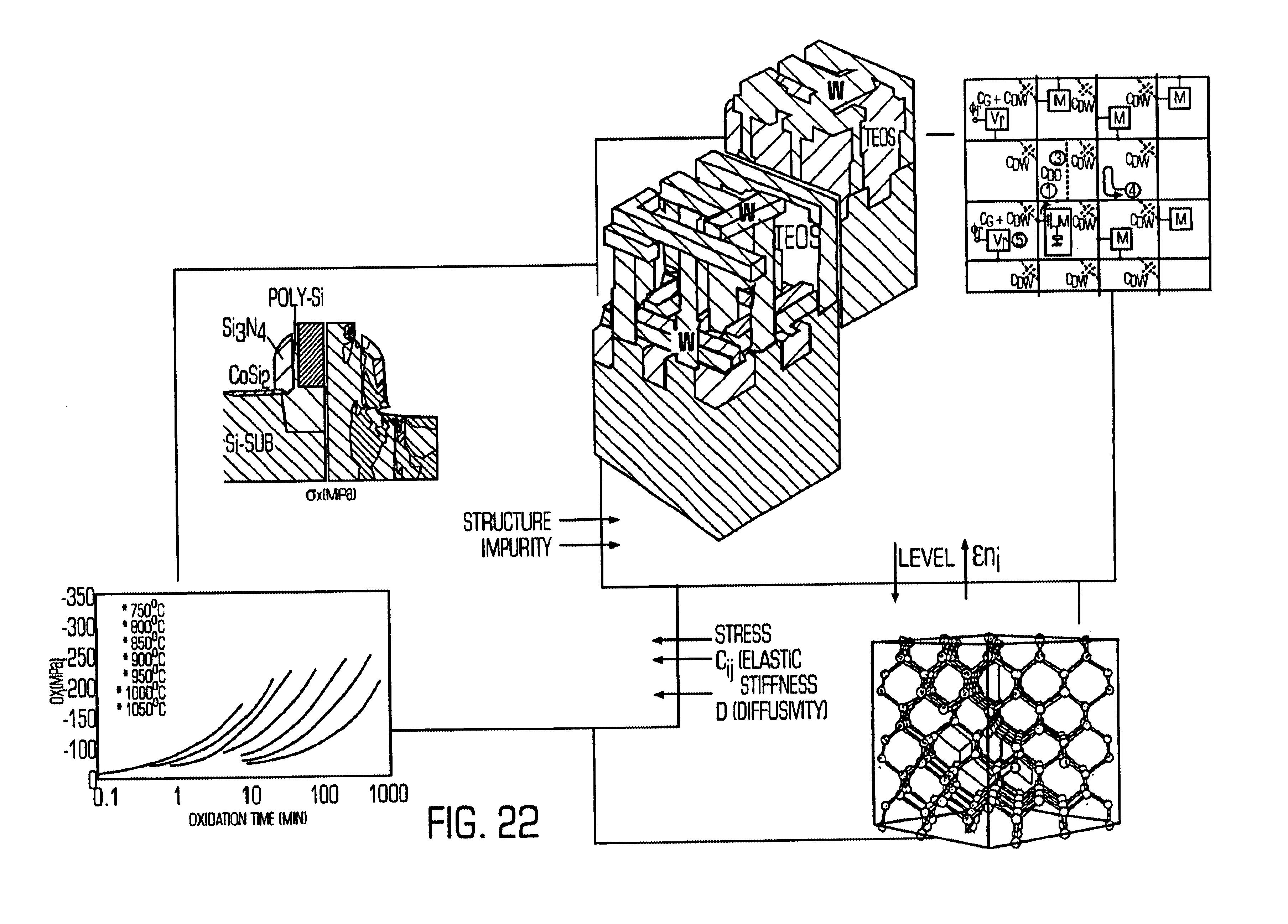
FIG. 21 shows a conceptual system overview of a simulator according to one embodiment of the present invention. The simulator system according to the present invention comprises a three-dimensional lumped device element simulation part, a three-dimensional visco-elastic process simulation part, and a material design part.

The three-dimensional lumped device element simulation part is interlinked with both the three-dimensional process simulation part and the material design part as shown in FIG. 21. The three dimensional process simulation part also is interlinked with the material design part.

The three-dimensional visco-elastic process simulation part comprises a visco-elastic model for silicon silicide, and SiO2, a non-equilibrium point-defect diffusion model, and an anisotropic Young modulus model. The three-dimensional visco-elastic process simulator can execute a metal deposition process, a metal etching process, a silicon substrate oxidation, a poly-silicon film oxidation, an i...


PUM


Abstract

An electronic device simulator includes a three-dimensional lumped device model, a three-dimensional visco-elastic process simulation model and a material design model that are interlinked with each other. The three-dimensional lumped device element model comprises a Poisson's equation model, an electron continuity equation model, a hole continuity equation model, a Maxwell's equations model, an eddy current equation model, and an Ohm's law equation model. The simulator accounts for the three dimensional characteristics of the circuit to determine circuit performance.

Description

1. Field of the InventionThe present invention relates to a semiconductor device manufacturing method, a semiconductor device, a semiconductor simulation method and a simulator, and more particularly to improve performance of lumped elements of devices and fabrication yield in scaled large scale integration (LSI), in conjunction with a computer aided design (CAD) tool.2. Description of the Prior ArtSemiconductor design and fabrication have a wide variety of issues, relating to LSI fabrication, process design, system design, device design, and so on. Problems underlying the current process / device / system design phase are described.First, a historical overview and the current status of the semiconductor industry and LSI device research and development phase are described. The semiconductor industry has continued to prosper as the result of continuous improvement of productivity and creative research throughout its history. It is believed that these trends will continue into the foresee...

Claims


Application Information

Patent Timeline
Patent Type & Authority Patents(United States)
IPC IPC(8): G06F17/50H01L21/28H01L21/00H01L21/3205H01L21/82H01L23/52
CPCG06F17/5018G06F2217/84H01L2924/0002H01L2924/00G06F30/23G06F2119/12
Inventor OKADA, TAKAKO
Owner KK TOSHIBA
Why Eureka
Try Eureka