Production method of III nitride compound semiconductor, and III nitride compound semiconductor element based on it
- Summary
- Abstract
- Description
- Claims
- Application Information
AI Technical Summary
Benefits of technology
Problems solved by technology
Method used
Image

Examples
first embodiment
[0050
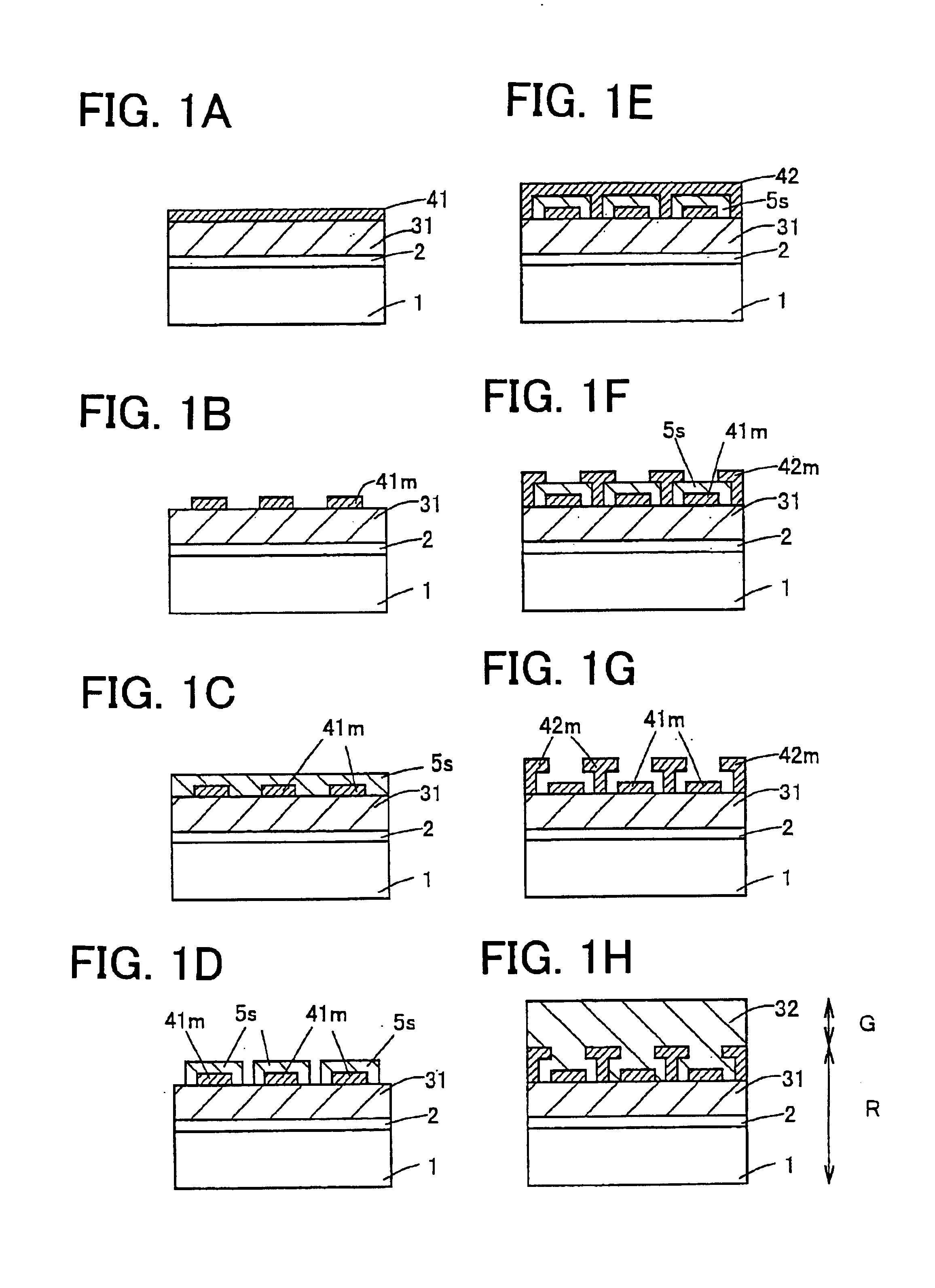
[0051]In the present embodiment, a buffer layer 2 and a Group III nitride compound semiconductor layer 31 as shown in FIGS. 1A-1H are employed. A monocrystalline sapphire substrate 1 containing an a-plane as a primary crystal plane was cleaned through organic cleaning and heat treatment. The temperature of the substrate 1 was lowered to 400° C., and H2 (10 L / min), NH3 (5 L / min), and TMA (20 μmol / min) were fed for about three minutes, to thereby form an AlN buffer layer 2 (thickness: about 40 nm) on the substrate 1. Subsequently, the temperature of the sapphire substrate 1 was maintained at 1000° C., and H2 (20 L / min), NH3 (10 L / min), and TMG (300 μmol / min) were introduced, to thereby form a GaN layer 31 (thickness: about 1 μm). Subsequently, SiNx was sputtered on the entire surface of the Group III nitride compound semiconductor layer 31, to thereby form a first mask material 41 having a thickness of about 100 nm (FIG. 1A). Then it was patterned in a stripe pattern each having ...
modified embodiment
[0060
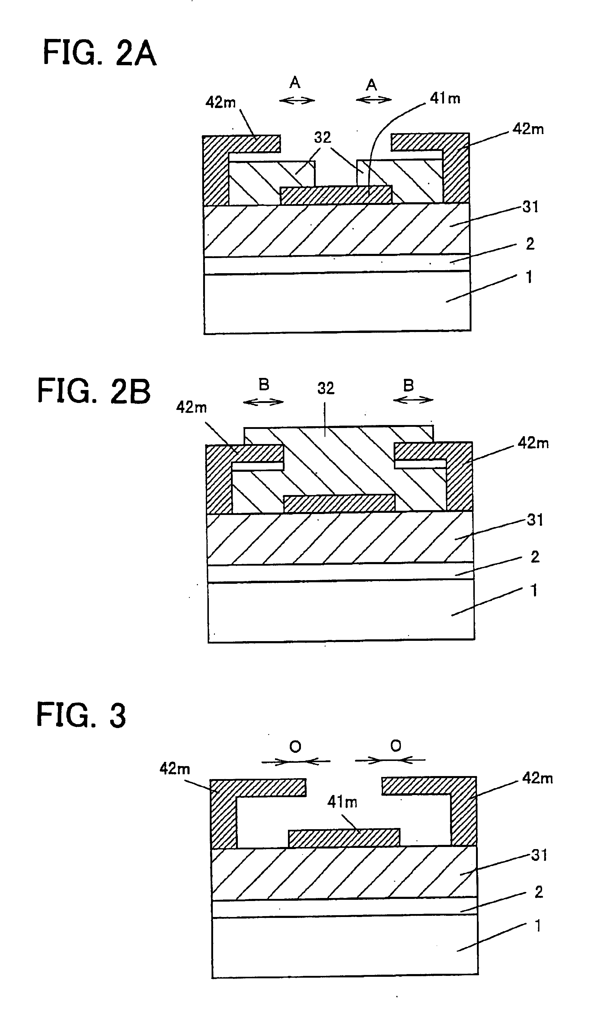
[0061]In the above embodiment, the first mask 41m and the second mask 42m are formed so as not to overlap with each other when the wafer is seen in the vertical direction from its top. Alternatively, an overlapped region represented by O as shown in FIG. 3, that is, the first mask 41m exists in the lower portion of the overlapped region and the second mask 42m exists in the upper portion thereof, can be formed. In the above embodiment, the limb of the second mask 42 was formed on the GaN layer 31 in stripe shape each having a width of 1 μm. Alternatively, a limb may be formed on the first mask 41m, and alternatively, the limb in a pillar shape may be formed on both the GaN layer 32 and the first mask 41m. Such limbs all depend on the design of the growth space of the GaN layer 32, and the second mask 42m may have a limb formed in an arbitrary shape according to the design of the growth space of the GaN layer 32.
second embodiment
[0062
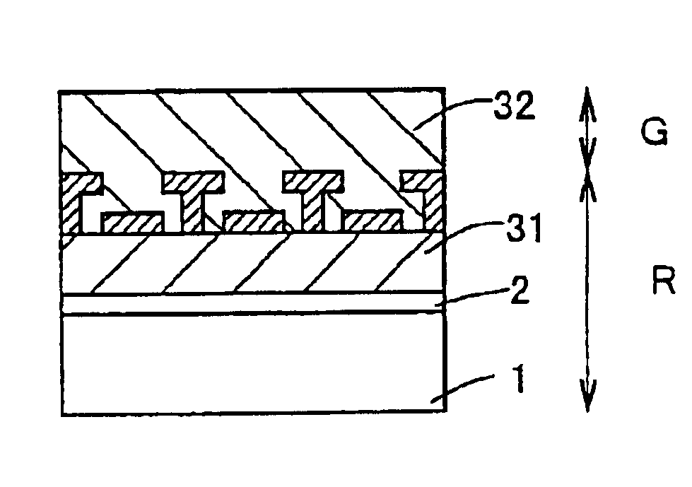
[0063]On a wafer formed in a manner similar to that of the first embodiment, a laser diode (LD) 1100 shown in FIG. 4 was formed in the following manner. Notably, in formation of the GaN layer 32, silane (SiH4) was introduced so as to form a silicon (Si)-doped n-type GaN layer serving as the GaN layer 32. For the sake of simplified illustration, the drawing merely illustrates a wafer 1000 (a region R in FIG. 1H) inclusively represent the sapphire substrate 1, the buffer layer 2, the GaN layer 31 and a portion of the GaN layer 32 which exists at the same level as the masks 41m and 42m, and GaN layer 103 (a region G in FIG. 1H) inclusively represent the other portion of the GaN layer 32.
[0064]A wafer 1000 which includes a sapphire substrate 1, an AlN buffer layer 2, the GaN layer 31, and a portion of the GaN layer 32 which exists at the same level as the masks 41m and 42m and the n-GaN layer 103 are formed. Successively, on the n-GaN layer 103, a silicon (Si)-doped Al0.08Ga0.92N n...
PUM
 Abstract
Description
Claims
Application Information
 - Generate Ideas
- Intellectual Property
- Life Sciences
- Materials
- Tech Scout
- Unparalleled Data Quality
- Higher Quality Content
- 60% Fewer Hallucinations
Browse by: Latest US Patents, China's latest patents, Technical Efficacy Thesaurus, Application Domain, Technology Topic, Popular Technical Reports.
© 2025 PatSnap. All rights reserved.Legal|Privacy policy|Modern Slavery Act Transparency Statement|Sitemap|About US| Contact US: help@patsnap.com