Bipolar transistor with graded base layer

a base layer and bipolar transistor technology, applied in the direction of thermoelectric device junction materials, electrical apparatus, semiconductor devices, etc., can solve the problems of conduction band spike at the emitter-base interface, limit the usefulness of devices for low power applications, etc., to reduce the injection of reverse holes, and improve the management of voltage budgets

Inactive Publication Date: 2005-01-25
IQE KC
View PDF19 Cites 21 Cited by
  • Summary
  • Abstract
  • Description
  • Claims
  • Application Information

AI Technical Summary

Benefits of technology

The reduction in turn-on voltage can result in better management of the voltage budget on both wired and wireless GaAs-based RF circuits, which are constrained either by standard fixed voltage supplies or by battery output. Lowering the turn-on voltage can also alter the relative magnitude of the various base current components in a GaAs-based HBT. DC current gain stability as a function of both junction temperature and applied...

Problems solved by technology

The turn-on voltage can limit the usefulness of devices for low power applications in which supply voltages are constrained by battery technology and the power requirements of other components.
HBTs, however, ca...

Method used


Image

  • Bipolar transistor with graded base layer
  • Bipolar transistor with graded base layer
  • Bipolar transistor with graded base layer

Examples


example 1

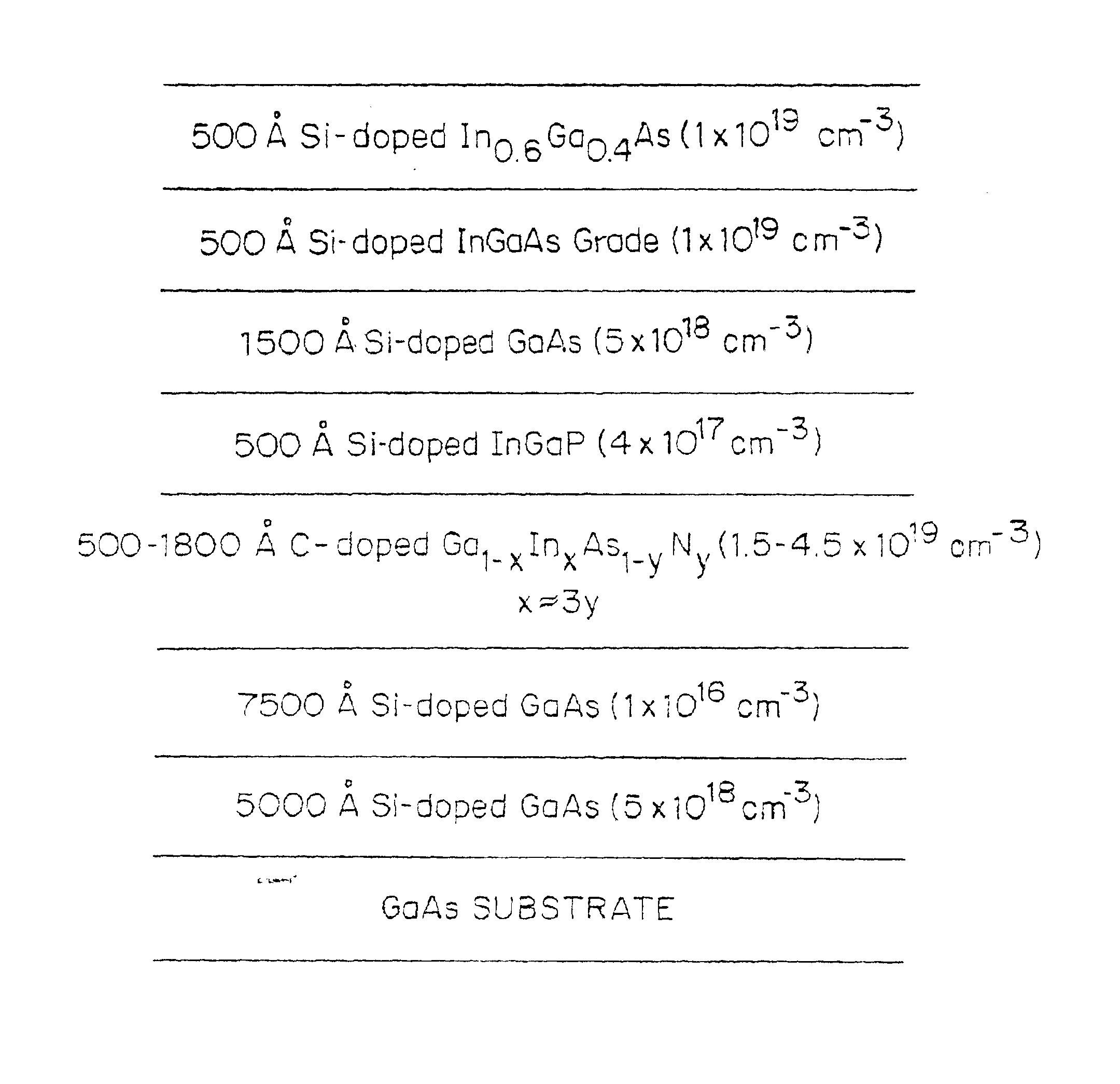
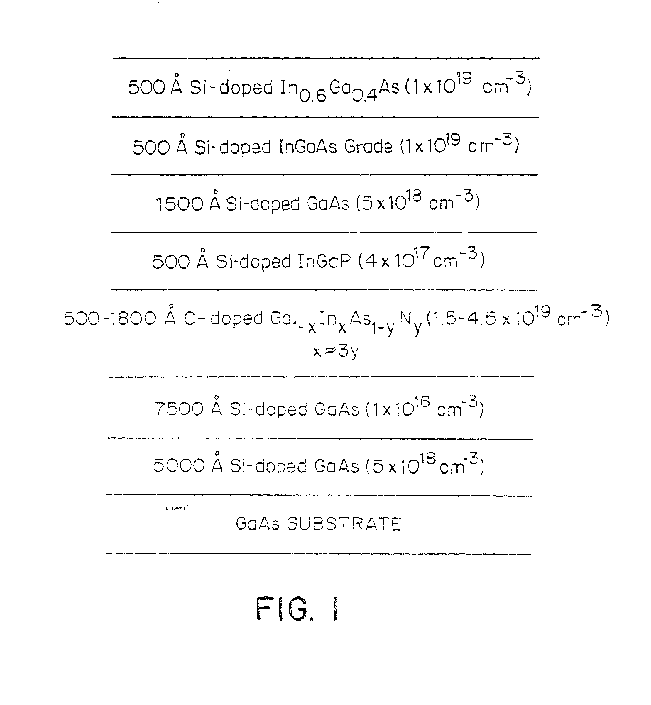
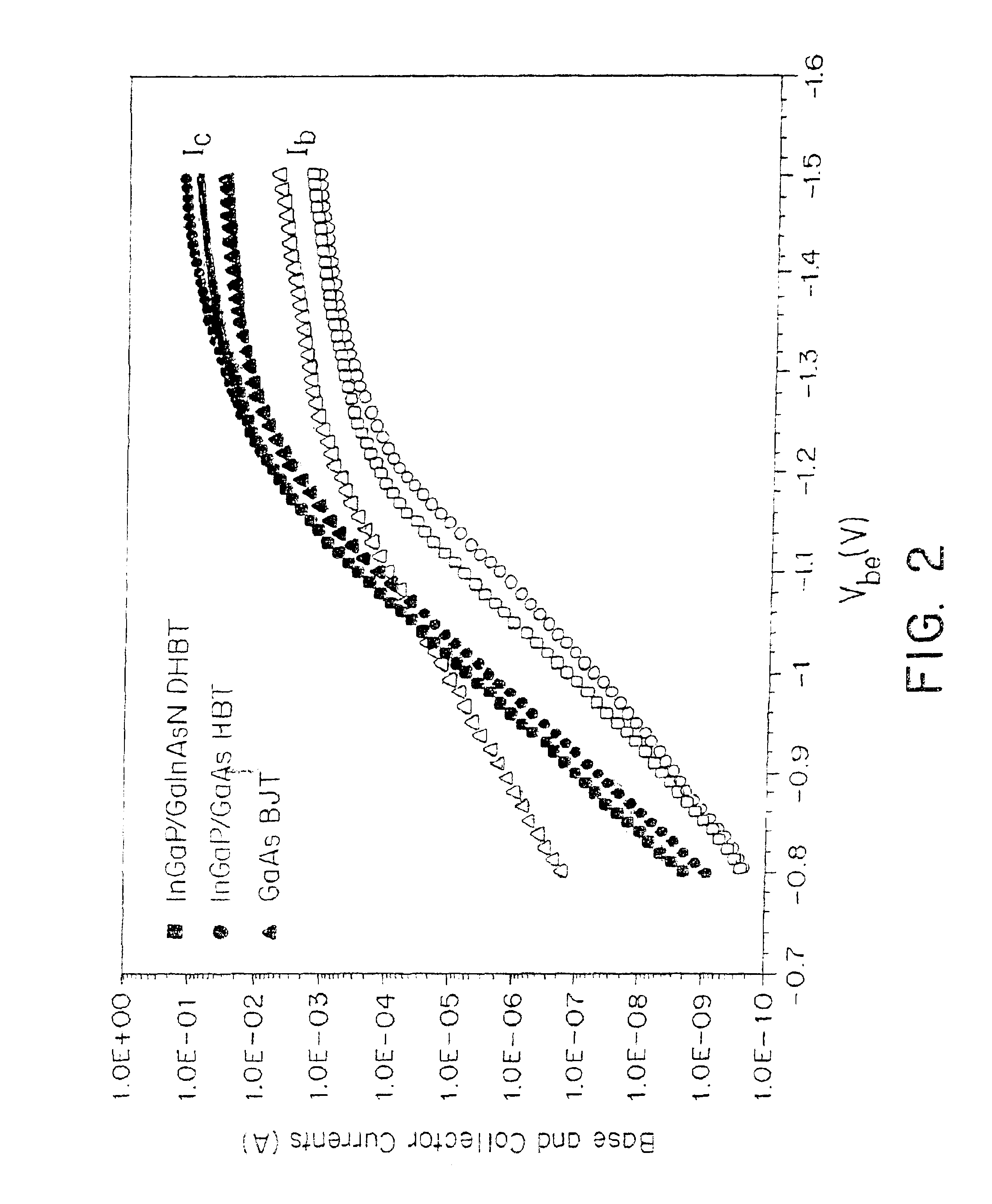
To illustrate the effect of reducing the band gap of the base layer and / or minimizing the conduction band spike at the emitter / base heterojunction, three different types of GaAs-based bipolar transistor structures were compared: GaAs emitter / GaAs base BJTs, InGaP / GaAs HBTs, and InGaP / GaInAsN DHBTs of the invention. A general representation of InGaP / GaInAsN DHBT structures used in the following experiments is illustrated in FIG. 1. There is only one heterojunction at the emitter / base interface since the base and the collector are both formed from GaAs. The GaAs base layer of the InGaP / GaAs HBT has a larger band gap than the base of the InGaP / GaInAsN DHBT. GaAs / GaAs BJTs have no heterojunctions since the emitter, collector and base are all made of GaAs. Thus, GaAs BJT structures are used as a reference to determine what impact, if any, a conduction band spike at the base-emitter interface has on the collector current characteristics of InGaP / GaAs HBTs. In the DHBTs of FIG. 1, InGaP is...

example 2

All of the GaAs devices used in the following discussion were MOCVD-grown, carbon-doped base layers in which the dopant concentration varied from about 3.0×1019 cm−3 to about 5.0×1019 cm−3 and a thickness which varied from about 500 Å to about 1500 Å, resulting in a base sheet resistivity (Rsb) of between 100 Ω / □ and 650 Ω / □. Large area devices (L=75 μm×75 μm) were fabricated using a simple wet-etching process and tested in the common base configuration. Relatively small amounts of indium (x˜1% to 6%) and nitrogen (y˜0.3%) were added incrementally to form two separate sets of InGaP / GaInAsN DHIBTs. For each set, growth was optimized to maintain relatively high, uniform carbon dopant levels (2.5×1019 cm−3), good mobility (˜85 cm2 / V-s), and high do current gain (>60 at Rsb˜300 Ω / square). The structure of a DFHBT used in the following experiments having a compositionally graded GaInAsN base layer is shown in FIG. 13. Alternative structures for DHBTs having compositionally garded base la...


PUM


Abstract

A semiconductor material which has a high carbon dopant concentration includes gallium, indium, arsenic and nitrogen. The disclosed semiconductor materials have a low sheet resistivity because of the high carbon dopant concentrations obtained. The material can be the base layer of gallium arsenide-based heterojunction bipolar transistors and can be lattice-matched to gallium arsenide emitter and/or collector layers by controlling concentrations of indium and nitrogen in the base layer. The base layer can have a graded band gap that is formed by changing the flow rates during deposition of III and V additive elements employed to reduce band gap relative to different III-V elements that represent the bulk of the layer. The flow rates of the III and V additive elements maintain an essentially constant doping-mobility product value during deposition and can be regulated to obtain pre-selected base-emitter voltages at junctions within a resulting transistor.

Description

BACKGROUND OF THE INVENTIONBipolar junction transistors (BJT) and heterojunction bipolar transistor (HBT) integrated circuits (ICs) have developed into an important technology for a variety of applications, particularly as power amplifiers for wireless handsets, microwave instrumentation, and high speed (>10 Gbit / s) circuits for fiber optic communication systems. Future needs are expected to require devices with lower voltage operation, higher frequency performance, higher power added efficiency, and lower cost production. The turn-on voltage (Vbe,on) of a BJT or HBT is defined as the base-emitter voltage (Vbe) required to achieve a certain fixed collector current density (Jc). The turn-on voltage can limit the usefulness of devices for low power applications in which supply voltages are constrained by battery technology and the power requirements of other components.Unlike BJTs in which the emitter, base and collector are fabricated from one semiconductor material, HBTs are fabr...

Claims


Application Information

Patent Timeline
IPC IPC(8): H01L21/02H01L21/331H01L29/02H01L29/10H01L29/66H01L29/737H01L29/20
CPCH01L29/1004H01L29/7371H01L29/66318H01L29/2003
Inventor WELSER, ROGER E.DELUCA, PAUL M.LUTZ, CHARLES R.STEVENS, KEVIN S.
Owner IQE KC
Why Eureka
Try Eureka