Supercharge Your Innovation With Domain-Expert AI Agents!

Low power integrating circuit for use with a photodetector and optical sensor including such an integrating circuit

a low-power, integrated circuit technology, applied in the direction of amplifiers, electric pulse generators, light-controlled amplifiers, etc., can solve the problems of insufficient solution, inability to realize the integrating capacitor as a standard mos transistor, etc., to maximize the maximum circuit output voltage, minimize the area (signal connections and transistors), and optimize the design

Inactive Publication Date: 2005-02-01
EM MICROELECTRONIC-MARIN
View PDF10 Cites 16 Cited by
  • Summary
  • Abstract
  • Description
  • Claims
  • Application Information

AI Technical Summary

Benefits of technology

Another advantage of the present invention resides in the fact that the circuit allows different voltages to be generated at the input and output during the reset phase, hence allows a voltage to be applied across the integrating voltage storage device (which is substantially equal to the photodetector bias voltage) which is sufficient for allowing the integrating voltage storage device to be formed of a capacitor-connected standard MOS transistor, the voltage being above the threshold voltage of such transistor.
resides in the fact that the circuit allows different voltages to be generated at the input and output during the reset phase, hence allows a voltage to be applied across the integrating voltage storage device (which is substantially equal to the photodetector bias voltage) which is sufficient for allowing the integrating voltage storage device to be formed of a capacitor-connected standard MOS transistor, the voltage being above the threshold voltage of such transistor.
Still another advantage of the invention resides in the fact that the integrating circuit may be operated at a low voltage in an optimal manner. Indeed, since the integrating circuit output is pulled during reset to a reference potential such as ground, while maintaining a sufficient voltage across the integrating voltage storage device, the integrating circuit output will ramp up from ground during integration (in case the photodetector is an n-well photodiode). The maximum circuit output voltage (with reference to ground) is thus defined by the allowable maximum output voltage ramp at the end of the integration. For a low-voltage supply, the maximum circuit output voltage can therefore be maximized resulting in a more optimal design.
In addition, the integrating circuit output typically drives subsequent signal processing blocks, which often consist of multiplexors and other switches. In order to minimize area (signal connections and transistors) in all on-chip circuitry, these switches need to be single transistor switches of small area. In a low supply voltage case, the gate drive of these switches must be able to get substantially above a threshold voltage above both the minimum (in this case ground) and the maximum signal swing (i.e. the maximum output voltage). Since the integrating circuit output ramps up from ground (still in the case of a n-well photodiode), this requirement can more easily be fulfilled with the circuit of the present invention.
Furthermore, it is usually difficult to fit a source-follower output stage into the feedback amplifier in order to lower the output impedance. Doing so generally requires an additional increase in the supply voltage, or a reduction in amplifier gain. If the output impedance is high, then compromises must be made in the following signal processing blocks, requiring additional circuitry, power or performance penalties. The present invention advantageously allows such a source-follower output stage to be used.

Problems solved by technology

A further disadvantage of the above passive type optical sensor resides in the fact that the integrating capacitance (defined in this case by the photodiode capacitance and the parasitic capacitance) is determined primarily by the photodiode size.
Accordingly, one disadvantage of the solution disclosed in U.S. Pat. No. 6,031,217 resides in the fact that it is not possible to realize the integrating capacitor as a standard MOS transistor, i.e. a MOS transistor having source and drain terminals connected together.
Poly or metal layers must therefore be used, which are very area-inefficient.
For applications requiring short response time and high collection efficiency, the solution proposed in U.S. Pat. No. 6,031,217 is therefore not adequate.
Another disadvantage of the above solution resides in the fact that the optical sensor requires two separate control lines (designated OSZERO and RUN in U.S. Pat. No. 6,031,217) for zeroing the operational amplifier and for controlling the timing of the integrating circuit.

Method used


Image

  • Low power integrating circuit for use with a photodetector and optical sensor including such an integrating circuit
  • Low power integrating circuit for use with a photodetector and optical sensor including such an integrating circuit
  • Low power integrating circuit for use with a photodetector and optical sensor including such an integrating circuit

Examples


Embodiment Construction

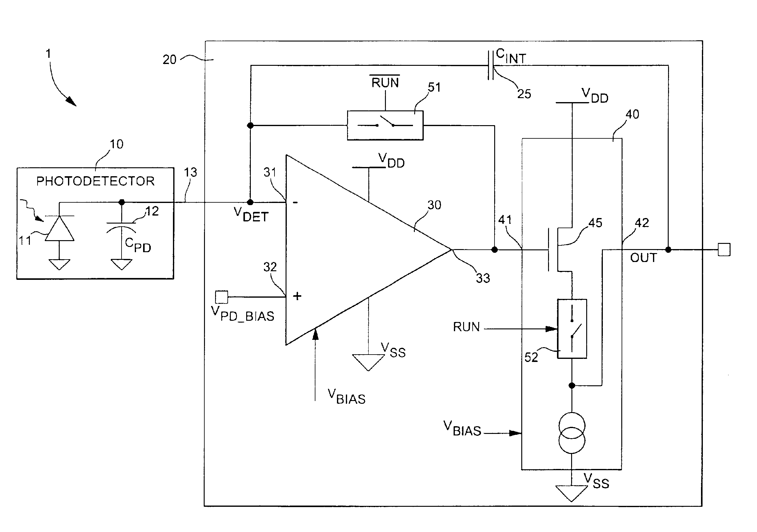
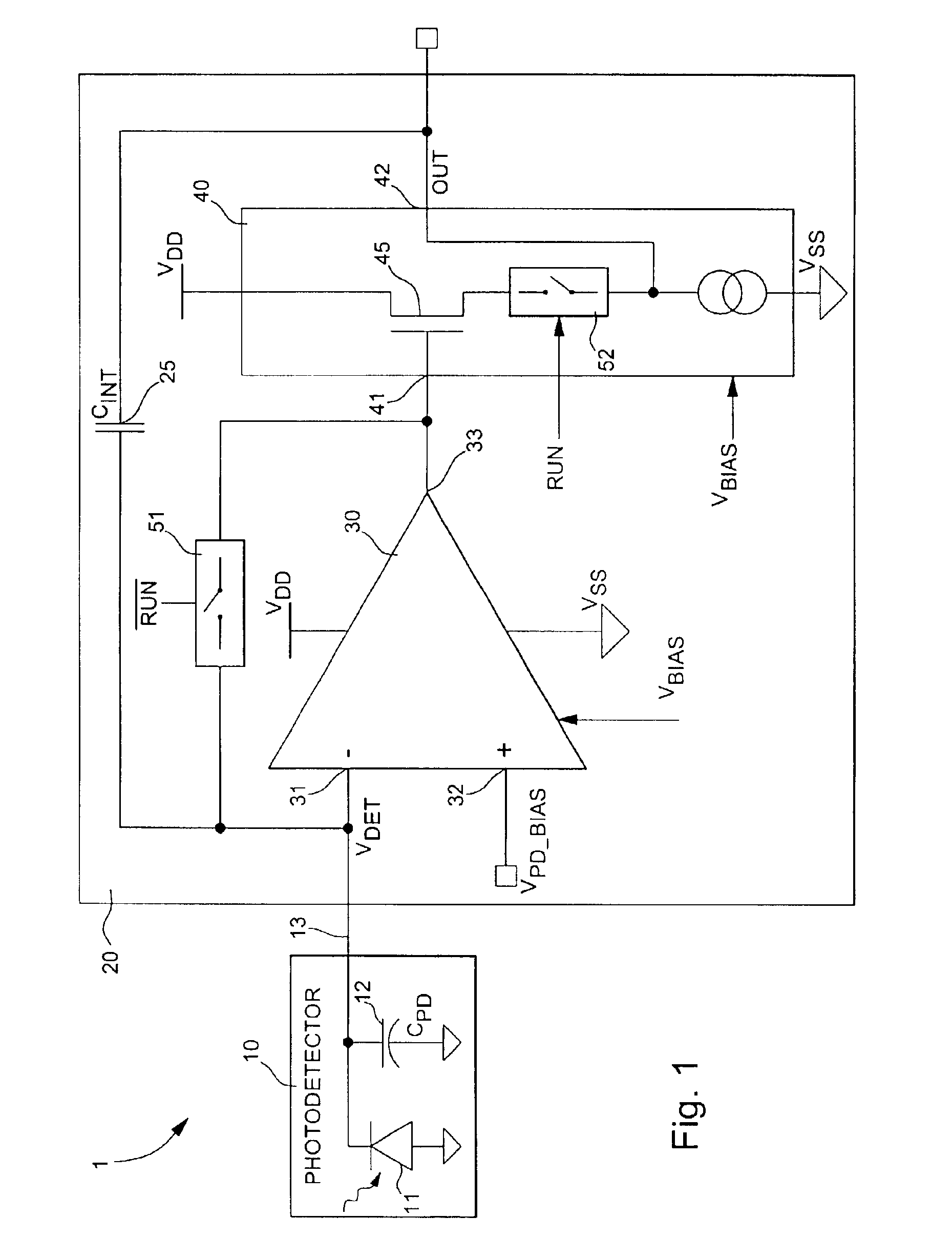
FIG. 1 is a generalized schematic bloc diagram of an optical sensor, indicated globally by reference numeral 1, including a photodetector 10 and an integrating circuit 20. The illustrated photodetector 10 here consists of a reverse-biased photodiode 11 (such as an n-well photodiode formed in a p-type semiconductor substrate). For the purposes of this description, the term “photodetector” includes any detector sensitive to radiant energy. Examples include in particular photodiodes, photo-gates and phototransistors. Reference numeral 12 denotes the photodiode capacitance CPD. Photodetector 10 has an output 13 which is coupled to integrating circuit 20.

Integrating circuit 20 includes an operational amplifier 30 having an inverting input 31 coupled to photodetector 10, a non-inverting input 32 coupled to a non-zero bias voltage VPD-BIAS, which set the desired photodiode reverse bias voltage, and an output 33. By way of non limiting illustration, the photodetector bias voltage is nominal...


PUM


Abstract

There is described an integrating circuit (20) for use with a photodetector (10) and an optical sensor (1) including such an integrating circuit. The integrating circuit comprises an operational amplifier (30) having a non-inverting input (32) connected to a non-zero bias voltage (VPD-BIAS), an inverting input (31) coupled to the photodetector (10), and at least one output (33). This integrating circuit further includes an integrating voltage storage device (25) having a first terminal coupled to the operational amplifier output and a second terminal coupled to the operational amplifier inverting input, and switching circuitry for controlling timing of the integrating circuit and switching the integrating circuit between a reset phase and an integration phase. The switching circuitry includes means (51, 52) for balancing the operational amplifier and developing a voltage across the integrating voltage storage device during the reset phase, which voltage is substantially equal to the bias voltage, the first terminal of the integrating voltage storage device being pulled to a reference potential (VSS) during this reset phase.

Description

FIELD OF THE INVENTIONThe present invention generally relates to optical sensors and more particularly to an integrating circuit and method for converting an input photo-generated current into an output voltage signal.BACKGROUND OF THE INVENTIONOptical sensors are used in a large number of applications such as scanning or digitising systems, optical pointing devices and imaging devices. Optical sensors generally operate by detecting electromagnetic radiation and producing an electrical signal that corresponds to the intensity of the electromagnetic radiation impinging on the optical sensor. Multiple optical sensors are generally used and are often geometrically positioned in arrays with individual optical sensor corresponding to a respective pixel of the array.Each optical sensor typically comprises a photodetector or photodetecting device, such as a photodiode or phototransistor, for converting electromagnetic radiation into an electrical signal. One specific type of optical sensor...

Claims


Application Information

Patent Timeline
IPC IPC(8): G01J1/44
CPCG01J1/44
Inventor LAUFFENBERGER, JAMES HAROLDBUESCHER, KEVIN SCOTT
Owner EM MICROELECTRONIC-MARIN
Features
  • R&D
  • Intellectual Property
  • Life Sciences
  • Materials
  • Tech Scout
  • Unparalleled Data Quality
  • Higher Quality Content
  • 60% Fewer Hallucinations
Learn More