Confinement device for use in dry etching of substrate surface and method of dry etching a wafer surface

a technology of confinement device and substrate, which is applied in the direction of electrical equipment, electrical discharge tubes, decorative arts, etc., can solve the problems of difficult dielectric etching, difficult to develop an optimized etching process that simultaneously clears, and undesirable non-planarity for subsequent photolithography patterning steps

Inactive Publication Date: 2005-02-08
BELL SEMICON LLC
View PDF9 Cites 13 Cited by
  • Summary
  • Abstract
  • Description
  • Claims
  • Application Information

AI Technical Summary

Problems solved by technology

The subsequent dielectric deposition process preserves this non-planarity of the wafer top surface but this non-planarity is undesirable for subsequent photolithography patterning steps.
In the case of patterning (photo and etch) after dielectric deposition, the requirement for simultaneously clearing the circuit areas and the alignment marks makes dielectric etching difficult.
For example, in dielectric via etching, it is difficult to develop an optimized etch process that simultaneously clears the vias and the alignment marks without over or underetching either.
Even if an optimized dielectric etch process could be developed, certain thicknesses of dielectric over the alignment marks may create undesirable interference effects, making their recognition by the stepper alignment system difficult.
Although CMP has a desired surface-planarization benefit (whether it is for dielectric or metal uniformity upon which successive layers can be built), an undesirable and costly side-effect of using CMP is that alignment marks required for subsequent photolithography steps are also “planarized”.
Currently, to clear-out alignment marks/recesses filled-in after a planarization process, such as CMP, IC manufacturers often use a series of additional costly (complex and time-consuming) photolithography steps: Applying a marker clear-out photo resist (or photosensitive coating that adheres to the outer surface of the wafer), exposing the resist to ult...

Method used


Image

  • Confinement device for use in dry etching of substrate surface and method of dry etching a wafer surface
  • Confinement device for use in dry etching of substrate surface and method of dry etching a wafer surface
  • Confinement device for use in dry etching of substrate surface and method of dry etching a wafer surface

Examples


Embodiment Construction

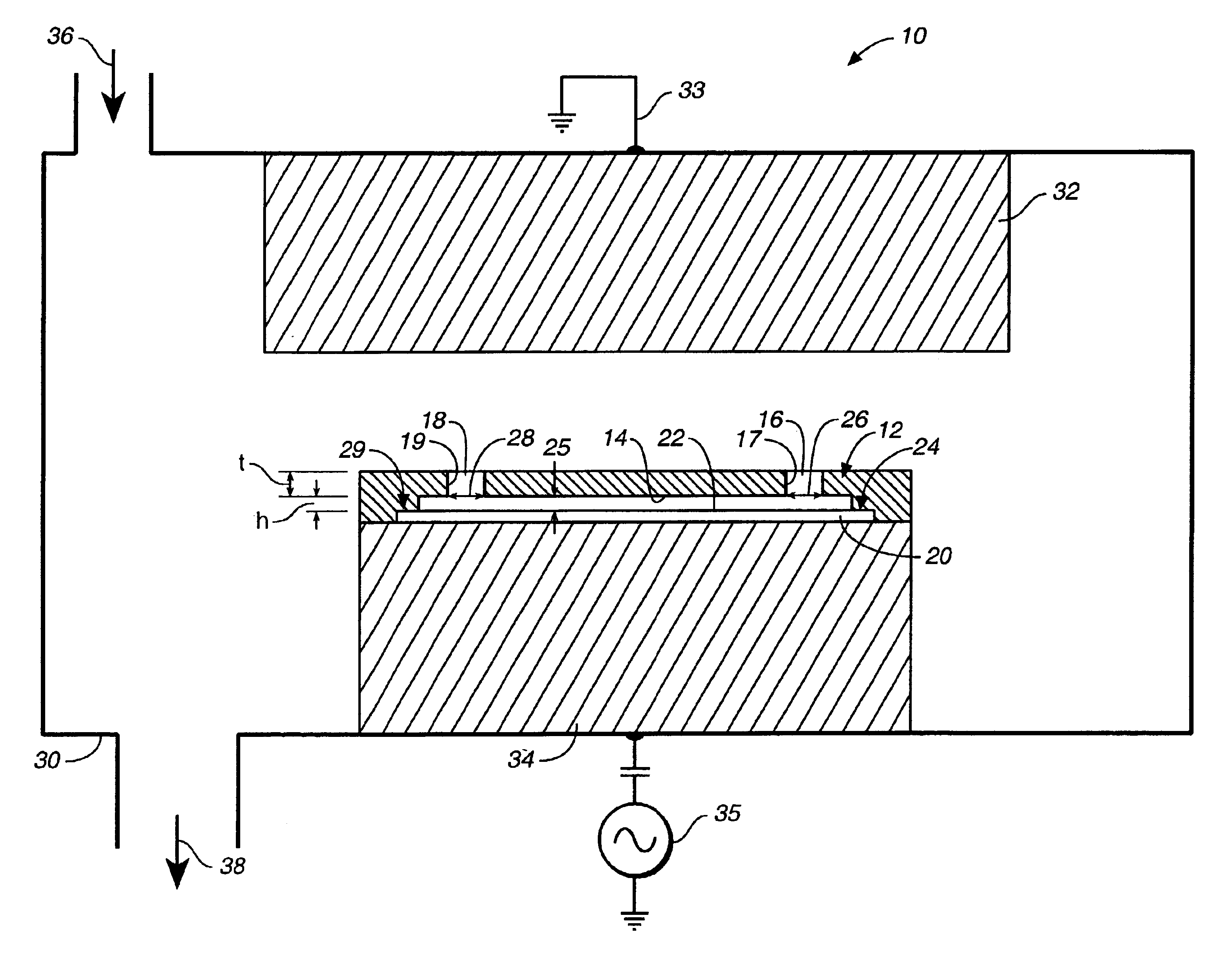
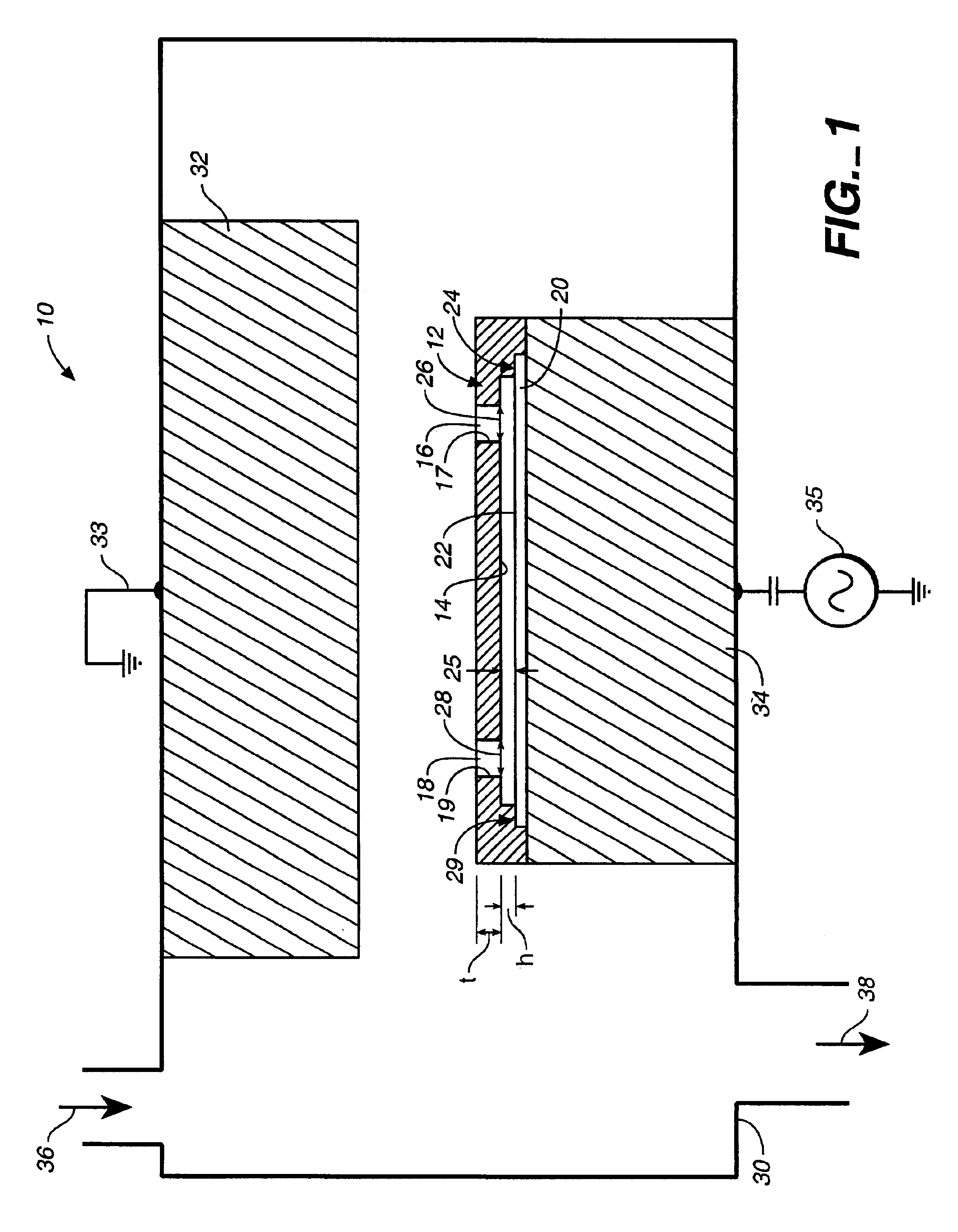
The preferred system 10 in FIG. 1 can be used for dry etching an integrated circuit (IC) wafer substrate. Arranged within the vacuum etching chamber (defined, schematically, by the block labeled 30) is a mechanically clamped chuck 34 for supporting wafer substrate 20, over which a lower surface 14 of preferred confinement device 12 has been positioned. At the shelf-areas identified and labeled 24 and 29 on the sectional view in FIG. 1, it is apparent that device 12 is in contact with the perimeter of substrate 20. In the event substrate 20 is an IC wafer, its perimeter will be circular as will be the contact shelf-area (24 / 29) of device 12.

As designed and unlike known dry etching systems and apparatuses, it is critical that gap-spacing 25 between lower surface 14 and top surface 22 of substrate 20 be such that a hollow cathode discharge can form within the channels 18 and 16 (and may extend slightly below) but will not otherwise form within the spacing 25. For this to happen, the ch...


PUM

PropertyMeasurementUnit
Lengthaaaaaaaaaa
Lengthaaaaaaaaaa
Thicknessaaaaaaaaaa

Abstract

A confinement device for operative arrangement within a substrate etching chamber, having a lower surface of the device generally arranged over a substrate outer top surface such that a gap-spacing therebetween is generally equidistant. This spacing is less than a sheath thickness for the plasma, preferably less than ⅓rd of an inner width of an aperture through the lower surface of the device. The aperture, sized preferably greater than 3 times the sheath thickness, is in communication with a channel of the device in which an etchant gas can be confined for reaction to selectively etch a localized area in the substrate outer top surface generally below the aperture. A system for dry etching an IC wafer includes a substrate etching chamber and a confinement device. The etchant gas may be a plasma induced and sustained by RF energy, a microwave source, or other source, as designed. And, a method is included for selectively etching a localized area in a substrate outer top surface, having the steps of: arranging a lower surface of a confinement device over the outer top surface, leaving a spacing therebetween, so that an aperture through said lower surface is located generally above the localized area (the spacing may cover the whole of the outer top surface, an area on which microcircuits are fabricated, or some other portion of the outer top surface); and providing an etchant gas to a channel in the device that is in communication with the aperture.

Description

BACKGROUND OF THE INVENTIONIn general, the present invention relates to devices and methods used in dry etching a surface of a wafer or substrate in semiconductor processing, and more particularly, to a novel dry etch confinement device that takes advantage of the so-called “hollow cathode effect” for operative arrangement within a substrate etching chamber apparatus that can be incorporated into an integrated cluster tool platform, if desired; and a novel method of dry etching a surface of a wafer substrate using such a confinement device with an etchant gas.Microelectronics is that area of electronics technology associated with the fabrication of electronic systems or subsystems using extremely small (microcircuit) components. Since semiconductor fabrication and processing is driven by the computer-electronics industry, the demands for greater capability and faster data processing of smaller-sized computerized systems result in a demand for smaller-and-smaller integrated circuit (...

Claims


Application Information

Patent Timeline
IPC IPC(8): H01J37/32
CPCH01J37/32623
Inventor JURGENSEN, CHARLES W.JOHNSON, GREGORY A.TARAVADE, KUNAL N.
Owner BELL SEMICON LLC
Why Eureka
Try Eureka