Process for high yield fabrication of MEMS devices

a technology of mems devices and fabrication processes, which is applied in the direction of photomechanical devices, soldering devices, instruments, etc., can solve the problems of reducing the yield of etching devices, reducing the etching accuracy and device yield, and requiring the use of thicker photoresists with reduced feature resolution, so as to achieve exceptionally precise layer to layer alignment of device components, the effect of reducing the thickness of the silicon device layer

Active Publication Date: 2005-03-29
TELEDYNE SCI & IMAGING
View PDF6 Cites 61 Cited by
  • Summary
  • Abstract
  • Description
  • Claims
  • Application Information

AI Technical Summary

Benefits of technology

The present invention provides a MEMS fabrication process that minimizes the thickness of the silicon device layers and the required etch times, provides exceptionally precise layer to layer alignment of the device components, does not require a wet etch to release the moveable device structure, employs a supporting substrate having no device features on one side, and utilizes low-temperature metal-metal bonding which is also less sensitive to environmental particulates than high temperature silicon-silicon oxide bonding. The process of the present invention can be used to fabricate a wide variety of MEMS devices, including sensors, but is particularly useful for fabrication of active MEMS devices (for example, electrical switches, variable capacitors and inductors, high frequency resonators, and mircromirrors for optical scanning and switching), which are often difficult to fabricate with high yield using prior art processes. Active MEMS devices typically use an electrostatic comb actuator but the process of the present invention could also be used to fabricate devices employing other types of actuators.

Problems solved by technology

Another significant disadvantage is that the through-wafer etching procedure used to open the optical path and provide access for removing the internal oxide layer greatly increases the processing time (3-5 hours), reduces the etching accuracy and device yield, and requires use of thicker photoresist with reduced feature resolution.
This wet chemical etching procedure is difficult to control and is another major source of yield loss.
In addition, the presence of deep etched features on both sides of the device complicates photolithographic processing and increases the likelihood of damage during handling.
Also, use of the stationary comb silicon layer as one of the electrical connections limits options for device integration and in some cases may necessitate extra processing to electrically ground or connect floating elements.
Furthermore, lack of precise alignment between the stationary and moveable comb structures for prior art processes further reduces the device yield and necessitates use of excessively high actuator voltages.
Although typical of the prior art MEMS fabrication processes, all of these disadvantages may not apply equally to every device and every fabrication process.

Method used


Image

  • Process for high yield fabrication of MEMS devices
  • Process for high yield fabrication of MEMS devices
  • Process for high yield fabrication of MEMS devices

Examples


Embodiment Construction

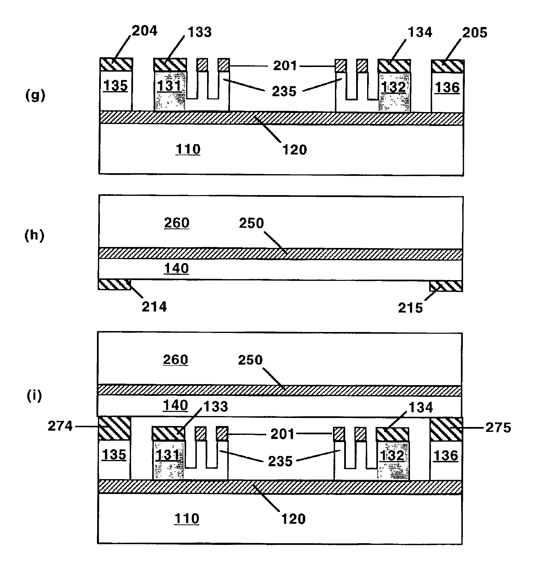
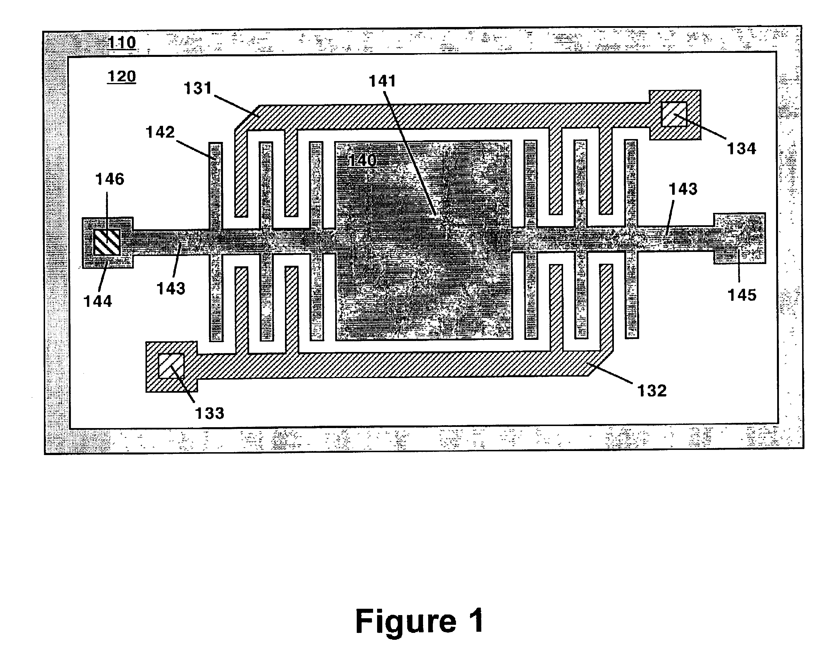
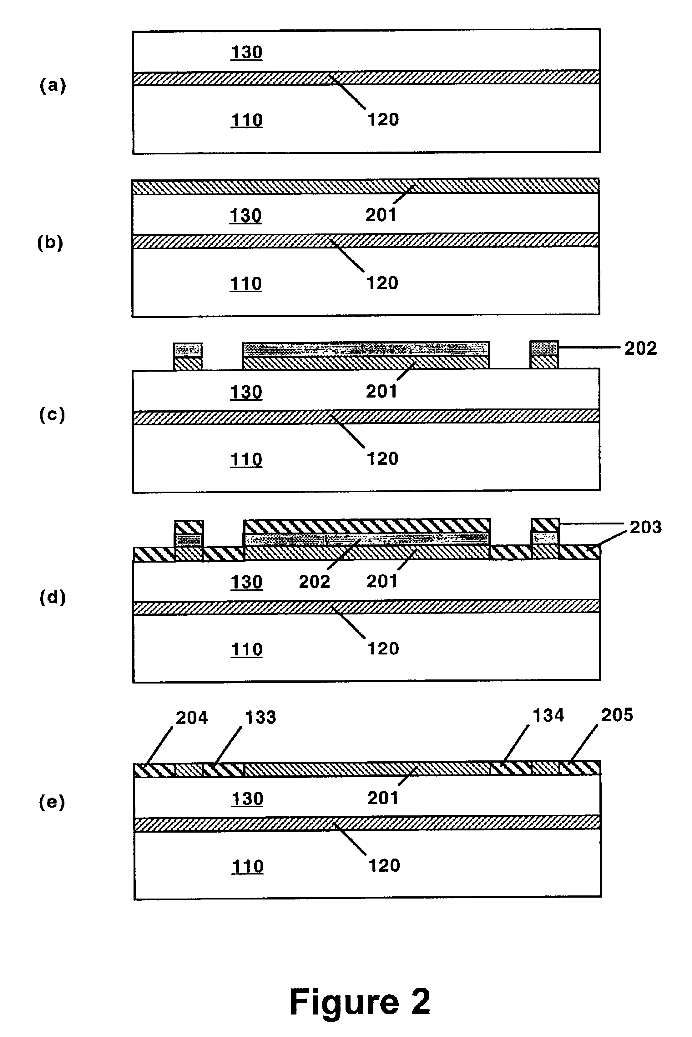
Terminology used in this document is generally the same as that used in the art. Patterning typically involves applying a thin layer of photoresist, exposing the photoresist to radiation through a mask having a predetermined pattern, and dissolving the uncured photoresist in a solvent so as to permit removal of the underlying substrate material, usually by etching. The photoresist may be negative (cured by exposure to radiation) or positive (degraded by exposure to radiation), and may be applied as a liquid by spraying, dipping or spin coating, for example, or as a dry film. As known to those skilled in the art, MEMS fabrication typically involves anisotropic etching of single crystal silicon wafers using silicon oxide as an etch stop, or as an etch resistant layer to prevent etching of underlying silicon. Silicon etching may be performed by wet chemical methods or dry methods (plasma etching, for example). Depending on the etching conditions, silicon or silicon oxide may be selecti...


PUM

PropertyMeasurementUnit
diameteraaaaaaaaaa
thickaaaaaaaaaa
thickaaaaaaaaaa

Abstract

A MEMS fabrication process eliminates through-wafer etching, minimizes the thickness of silicon device layers and the required etch times, provides exceptionally precise layer to layer alignment, does not require a wet etch to release the moveable device structure, employs a supporting substrate having no device features on one side, and utilizes low-temperature metal-metal bonding which is relatively insensitive to environmental particulates. This process provided almost 100% yield of scanning micromirror devices exhibiting scanning over a 12° optical range and a mechanical angle of ±3° at a high resonant frequency of 2.5 kHz with an operating voltage of only 20 VDC.

Description

BACKGROUND OF THE INVENTION1. Field of the InventionThis invention is concerned with micro-electro-mechanical systems (MEMS) and in particular with processes for fabricating MEMS devices.2. Description of the Related ArtMicro-electro-mechanical systems (MEMS) fabricated from single crystal silicon by anisotropic etching are widely used for sensors (accelerometers, for example) and are of increasing commercial interest and importance for use in a variety of active devices, such as electrical switches, variable capacitors and inductors, and micromirrors for optical scanning and switching. A typical MEMS active device comprises a functional element that is anchored by a spring or hinge but suspended above a substrate so that it can be moved by an actuator, such as a capacitively driven comb structure. The moveable functional element might be a switch contact, capacitor plate or micromirror, for example. In addition to the small size desirable for portable equipment, MEMS devices offer ...

Claims


Application Information

Patent Timeline
Patent Type & Authority Patents(United States)
IPC IPC(8): B81C5/00G02B26/08B81C99/00
CPCG02B26/0833B81C99/0065
Inventor TSAI, CHIALUN
Owner TELEDYNE SCI & IMAGING
Why Eureka
Try Eureka