Incoherent light-emitting device apparatus for driving vertical laser cavity
- Summary
- Abstract
- Description
- Claims
- Application Information
AI Technical Summary
Benefits of technology
Problems solved by technology
Method used
Image

Examples
example 1
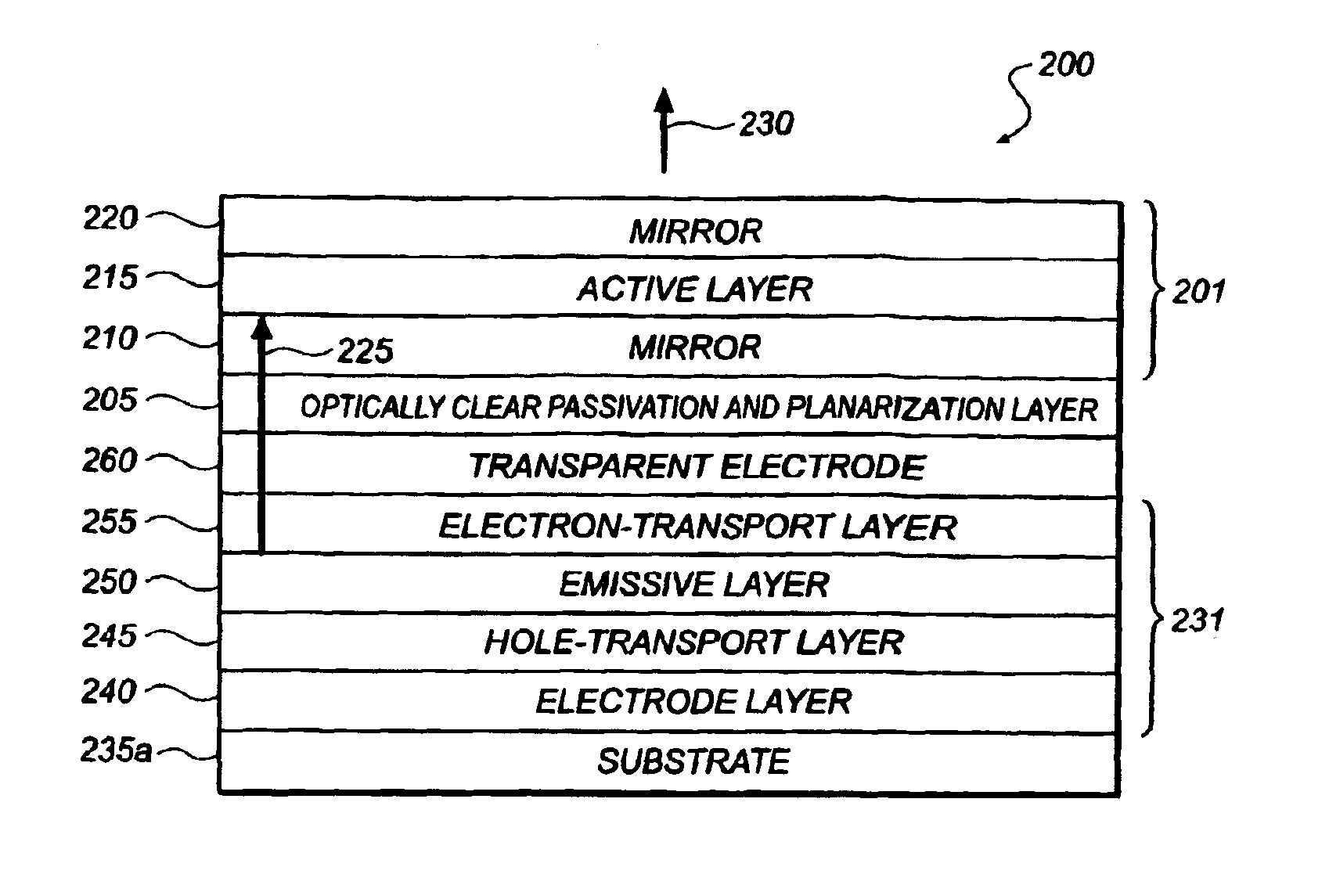
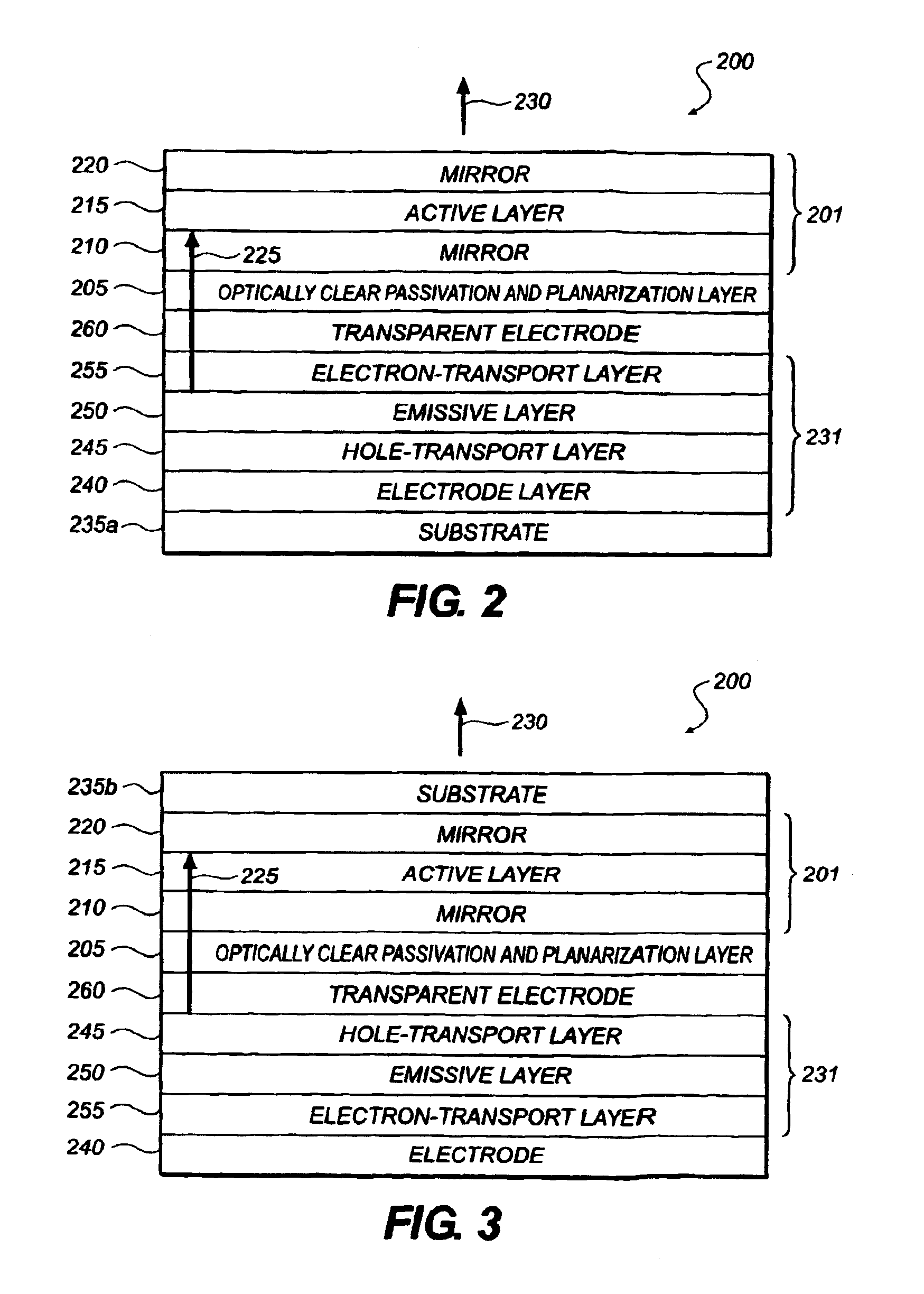
In order to determine the general lasing characteristics of the organic solid-state laser device described in FIGS. 2 and 3, a vertical laser cavity structure was formed on a pre-cleaned 4-inch Si substrate. Over the substrate was deposited by conventional e-beam deposition the bottom DBR mirror, which was composed of alternating high and low refractive index layers of Ta2O5 and SiO2, respectively. The resulting mirror had a greater than 99% reflectance stop band between 600 and 720 nm, where at the center wavelength of 660 nm its reflectivity was greater than 99.999%. On the top of the bottom DBR mirror was deposited by high vacuum thermal evaporation the active layer composed of 200 nm of Alq doped with 1% of DCJTB. Lastly, the top DBR mirror was deposited by low temperature e-beam deposition, such that the measured temperature of the Si substrate was kept below 72° C. It was composed of alternating high and low refractive index layers of TiO2 and SiO2, respectively. The resulting...
example 2
In this example vertical laser cavity structures analogous to those described in Example 1 will be discussed. Three cavities (with Si substrates) were constructed which nominally were designed to lase at 660 nm. Cavity A had an active layer thickness of λ1 / 2n (=195 nm), cavity B had an active layer thickness of λ1 / n (=390 nm), and cavity C had an active layer thickness of 2λ1 / n (=780 nm). All three active layers were composed of Alq doped with 1% of DCJTB. The top and bottom DBR mirrors were the same in all three cases and were constructed as follows. The bottom DBR mirror was composed of alternating high and low refractive index layers of TiO2 and SiO2, respectively. The resulting mirror had a greater than 99% reflectance stop band between 580 and 750 nm, where at the center wavelength of 665 nm its reflectivity was greater than 99.999%. In addition, the mirror had a broad reflectance maximum centered at 445 nm, whose peak reflectance was greater than 92%. The top DBR mirror was al...
example 3
This is an example of the embodiment given in FIG. 2, where the incoherent light output 225 from an organic light-emitting diode 231 is used to drive a vertical laser cavity 201. Cavities A and B, as described in Example 2, were used as the vertical laser cavity structures, while the OLED device was constructed as follows:
a) a 85 nm thick transparent anode of ITO-coated glass was ultrasonicated in a commercial detergent, rinsed in deionized water, degreased in toluene vapor, and contacted by a strong oxidizing agent;
b) a 150 nm thick NPB hole-transport layer was deposited over the ITO anode by conventional thermal vapor deposition;
c) a 30 nm thick ADN light-emitting layer was deposited over the NPB layer by conventional thermal vapor deposition;
d) a 20 nm thick Alq electron-transport layer was deposited over the light-emitting layer by conventional thermal vapor deposition;
e) a 100 nm thick Mg-Ag cathode was deposited over the electron-transport layer by conventional thermal vapor d...
PUM
 Abstract
Description
Claims
Application Information
 - R&D
- Intellectual Property
- Life Sciences
- Materials
- Tech Scout
- Unparalleled Data Quality
- Higher Quality Content
- 60% Fewer Hallucinations
Browse by: Latest US Patents, China's latest patents, Technical Efficacy Thesaurus, Application Domain, Technology Topic, Popular Technical Reports.
© 2025 PatSnap. All rights reserved.Legal|Privacy policy|Modern Slavery Act Transparency Statement|Sitemap|About US| Contact US: help@patsnap.com