

Near-field optical probe
a near-field optical and probe technology, applied in the field of near-field optical probes, can solve the problems of increasing the size of the microscope and its complexity, the minimum unit of analysis sample structure is limited to several hundred nanometers, and the optical microscope used for observing the optical characteristic distribution of a sample cannot realize structural observation with a resolving power, etc., to achieve efficient collection
- Summary
- Abstract
- Description
- Claims
- Application Information
AI Technical Summary
Benefits of technology
Problems solved by technology
Method used
Image

Examples
embodiment 1
[Embodiment 1]
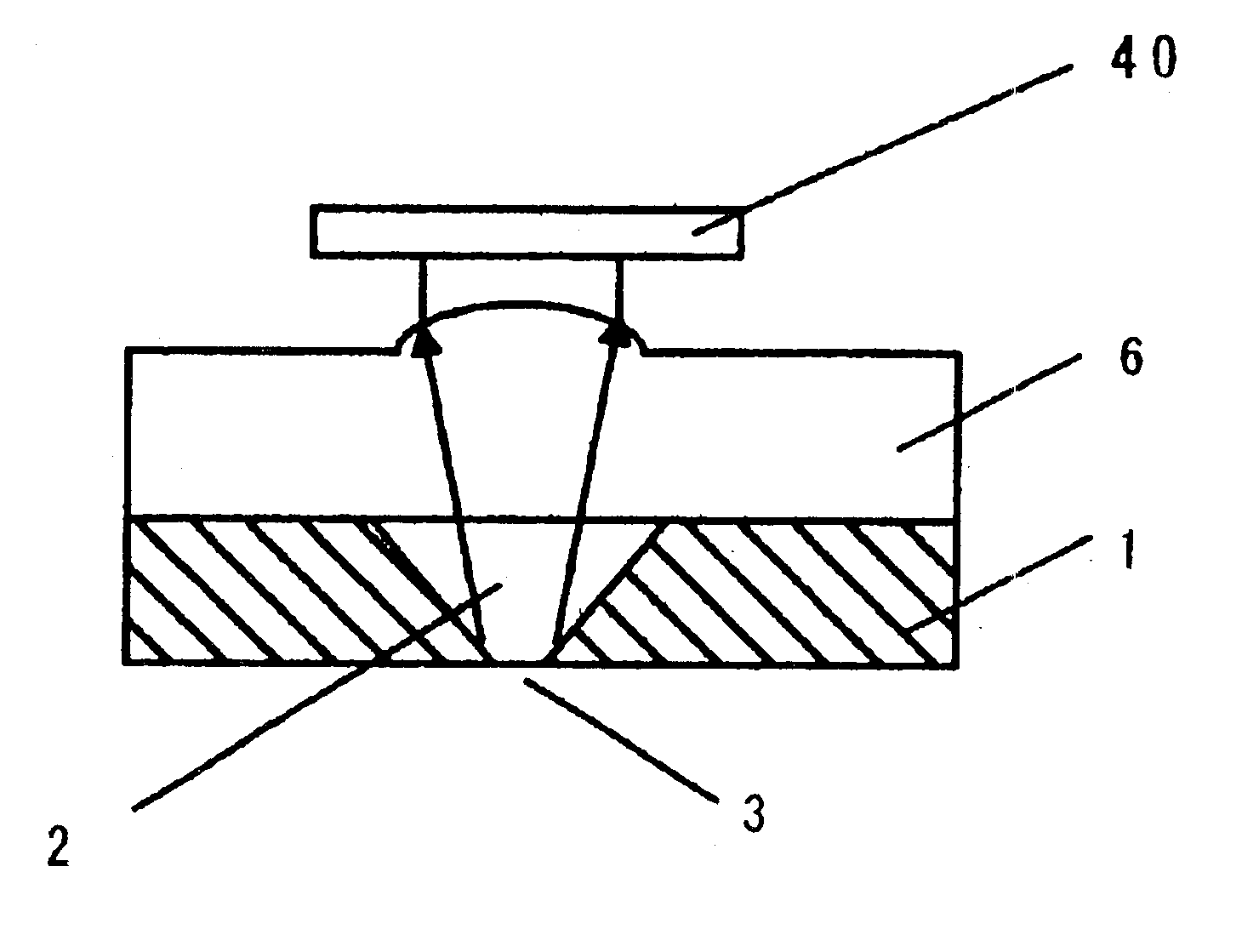
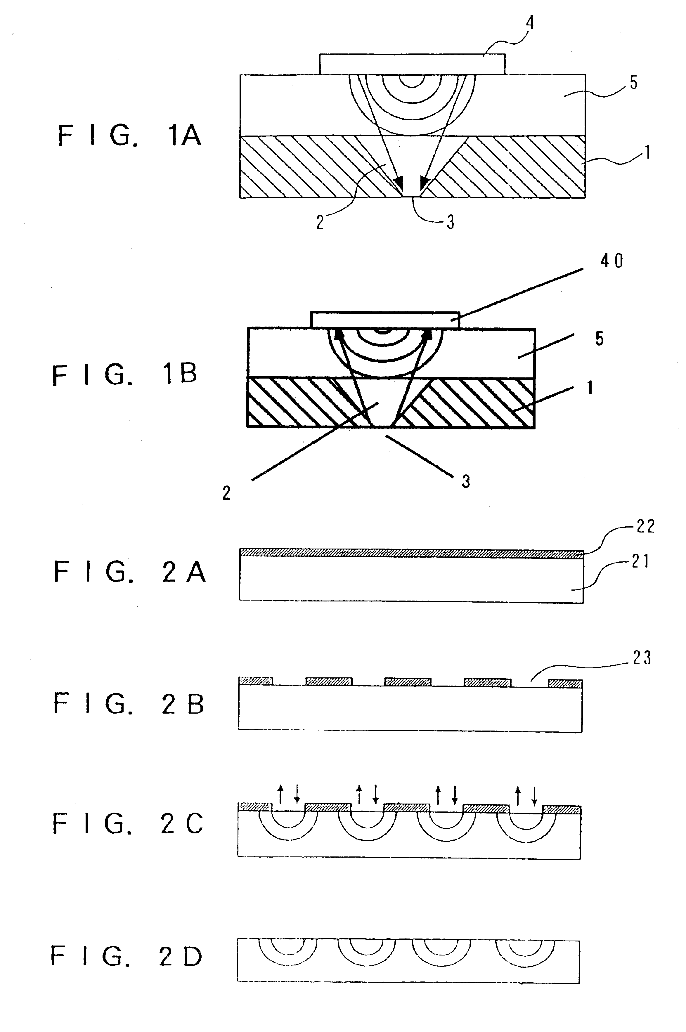
[0054]FIG. 1A shows a sectional view of one part of a near-field optical probe according to Embodiment 1.
[0055]In FIG. 1A, a silicon substrate 1 with an aperture 3 has a planar microlens 5 wherein a surface emitting laser 4 is further provided on the planar microlens 5.
[0056]The silicon substrate 1 is formed with a taper portion 2 in a manner penetrating through it, to have a microscopic aperture 3. The aperture 3 has a diameter, for example, of 50 nanometers so that a near field can be generated by the light introduced through the taper portion 2. The taper portion 2 is formed by microlithography using conventional photolithography or silicon anisotropic etching. For example, a silicon substrate 1 having a (100) plane at both surfaces is formed by thermal oxide films or Au / Cr metal films as masks for anisotropic etching to be subsequently conducted. The mask on one of the surfaces is partially removed to form an aperture window, thereby exposing the (100) plane. Subse...
embodiment 2
[Embodiment 2]
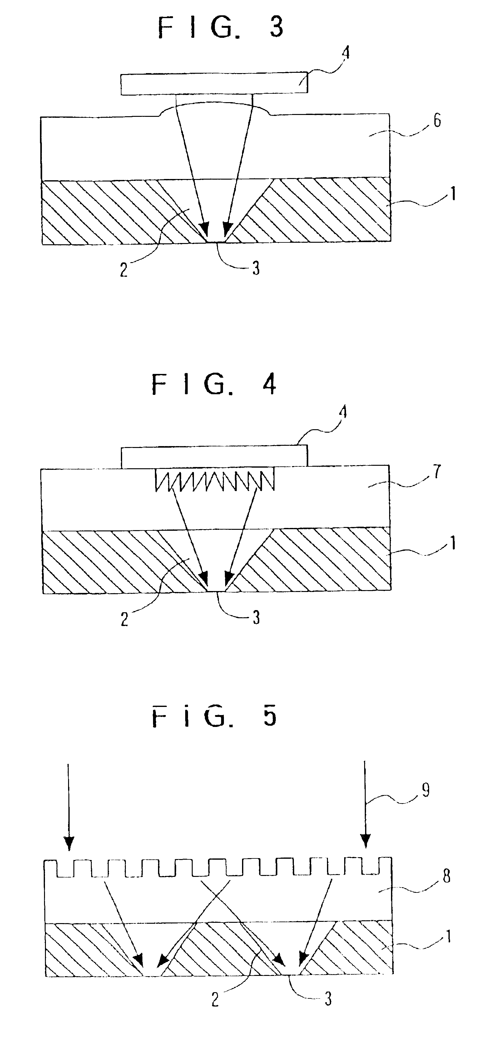
[0072]FIG. 3 shows a sectional view of one part of a head for an optical memory according to Embodiment 2.
[0073]In FIG. 3, a microlens substrate 6 is arranged in place of the planar microlens 5 of FIG. 1 explained in Embodiment 1.
[0074]In the microlens substrate 6, in a selective ion exchange method similar to that explained in Embodiment 1, ions large in radius are diffused into the glass substrate and are selected to cause a swell at a circular aperture portion due to a difference in diameter of ions to be exchanged. Accordingly, a lens is made in a usual lens shape, different from the gradient refractive index created as a result of selective ion exchange in Embodiment 1. Due to this swell, the microlens substrate 6 is not flat in its surface so that surface emitting laser 4 cannot be arrange directly thereon. Consequently, there is a necessity to provide a distance between the microlens substrate 6 and the surface emitting laser 4. A not-shown spacer is used in fix...
embodiment 3
[Embodiment 3]
[0080]In FIG. 4, a Fresnel zone plate 7 is arranged in place of the planar microlens 5 of FIG. 1 explained in Embodiment 1. The Fresnel zone plate 7 is used to create diffraction light by a fine pattern on a glass substrate to cause a lens effect. It is possible to collect the coherent light given from the surface emitting laser 4 in the aperture 3 without aberration. The fine processing for the Fresnel zone plate 7 can use various method including electron beam processing, laser interference method, dry etching method and fine machining. However, if a master is made, mass production is possible by stamping or the like.
[0081]The provision of a Fresnel zone plate between the surface emitting laser as a light source and the aperture can increase the intensity of a near field to be generated or detected in the aperture.
[0082]Incidentally, a holographic lens 8 may be used as shown in FIG. 5, in place of the Fresnel zone plate 7. The holographic lens 8 is a hologram formed ...
PUM
| Property | Measurement | Unit |
|---|---|---|
| diameter | aaaaa | aaaaa |
| refractive index | aaaaa | aaaaa |
| refractive index | aaaaa | aaaaa |
Abstract
Description
Claims
Application Information