Field effect transistor and manufacturing method therefor

a field effect transistor and manufacturing method technology, applied in the field of field effect transistors, can solve the problems of insufficient thickness of electrodes, inability to form electrodes with sufficient thickness, inability to make electrode resistance sufficiently small, etc., to achieve satisfactory power characteristics, small electrode resistance, and the effect of small electrode resistan

Inactive Publication Date: 2005-05-24
FURUKAWA ELECTRIC CO LTD
View PDF17 Cites 26 Cited by
  • Summary
  • Abstract
  • Description
  • Claims
  • Application Information

AI Technical Summary

Benefits of technology

[0034]Another object of the present invention is to provide an FET which is excellent in power characteristics and which can be fabricated by simplified processes at low costs, and a manufacturing method therefor.
[0038]According to the present invention, electrodes of a field effect transistor are formed by electrode materials filled into through openings formed in an insulating resin film, and therefore, the electrodes can be made thick to the extent that the field effect transistor has a sufficiently small electrode resistance, whereby the on-resistance of the transistor can be sufficiently small, and a satisfactory power characteristic can be achieved. In addition, by filling the same electrode material into the through openings for electrode formation, the field effect transistor can be fabricated at low costs with simplified fabrication processes.
[0039]According to the present invention, a field effect transistor can be fabricated in the form of a layered structure comprised of a channel layer vertically sandwiched between source and drain regions. With such a field effect transistor in which the channel length (i.e., the length of the channel layer) corresponds to the thickness of the channel layer, the channel length can be made sufficiently short to make the on-resistance sufficiently small by variably controlling the thickness of the channel layer because the accuracy of thickness control for the channel layer is higher than the dimensional accuracy of a resist pattern conventionally used for channel layer formation.

Problems solved by technology

In conventional GaN-based FETs, however, since a lift-off method is adopted for electrode formation, it is difficult to form electrodes with a sufficient thickness so as to make electrode resistance sufficiently small.
FETs have their on-resistance determined by electrode resistance as well as contact resistance between electrodes and corresponding respective regions of the FETs, and therefore, the on-resistance cannot be made sufficiently small, if the electrode resistance is not small.
Thus, the electrode resistance cannot be made sufficiently small, especially for a large-area device, posing a problem that it is difficult to attain satisfactory power characteristics.
Accordingly, photolithography, etching and vapor-depositing processes for the lift-off method must be repeated, causing a problem of increased costs due to complicated fabrication processes.
In addition, usage of highly hard sapphire substrate 50 poses a further problem that a difficult is encountered in properly cutting a wafer-into chips in the dicing process which is the final wafer process.
Moreover, the sapphire substrate 50 is extremely poor in heat dissipation, making it difficult for a power device to dissipate heat generated therein.
This causes problems of deterioration of electrodes and of badly affecting on characteristics such as drain withstand voltage, on-resistance and the like.
However, a method for epitaxial growth of a GaN layer on a silicon substrate has not been established as yet.
Due to the difficulty in sufficiently decreasing the channel length, the conventional GaN-based MISFET entails a drawback that the on-resistance cannot be made sufficiently small despite that the bandgap of p-type GaN constituting the channel layer 152 is wider than those of Si and GaAs.
Nevertheless, a suitable device structure that effectively utilizes such an advantage of wide bandgap semiconductors has not been proposed as yet.

Method used


Image

  • Field effect transistor and manufacturing method therefor
  • Field effect transistor and manufacturing method therefor
  • Field effect transistor and manufacturing method therefor

Examples


example

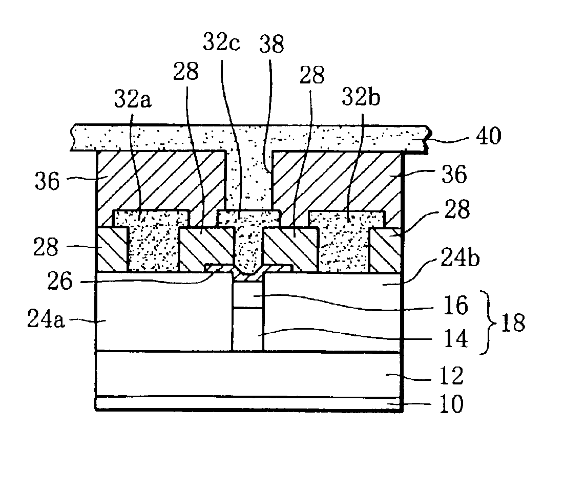
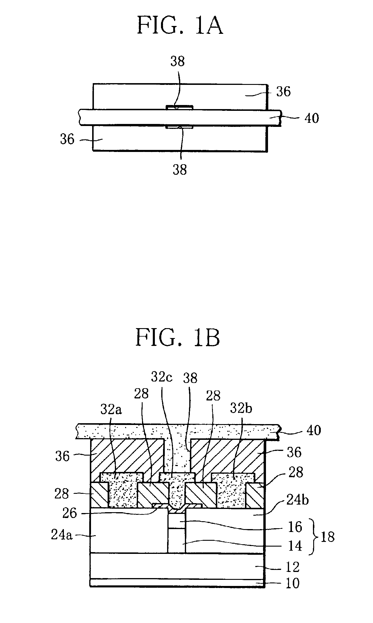
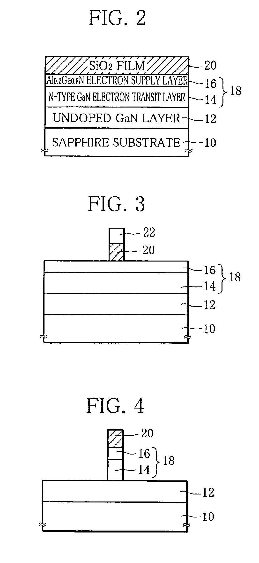
[0145]With reference to FIGS. 25-36, an example of a method for manufacturing a GaN-based MISFET according to the second embodiment will be explained.

[0146]First, a series of crystal growth on a semi-insulating sapphire substrate 110 was done by means of a gas source molecular beam epitaxy (MBE) method using an ultra-high vacuum growth apparatus.

[0147]More specifically, a GaN buffer layer (not shown) of 50 nm thick was grown at a growth temperature of 640° C., using as raw material gases, gallium (Ga) at a partial pressure of 4×10⁻⁵ Pa and radical nitrogen (N) at a partial pressure of 4×10⁻⁴ Pa. Then, at a growth temperature of 850° C., an undoped GaN layer 112 of 1000 nm thick was grown using Ga and N at partial pressures of 1.33×10⁻³ Pa and 6.65×10⁻³ Pa, respectively.

[0148]In succession, an n-type GaN drain layer 114 of 200 nm thick with carrier concentration of 1×1019 cm−3 was grown at a growth temperature of 850° C., using Ga and N at partial pressures of 6.65×10⁻³ Pa and 6.65×1...


PUM


Abstract

GaN-based FET has a sapphire substrate of about 50 nm thick on which an n-type GaN electron transit layer and an Al0.2Gao0.8N electron supply layer are formed, together with n+-type GaN contact regions sandwiching the electron transit and supply layers therebetween. On the entire faces of these layer and regions is formed a polyimide interlayer insulating film of about 3000 nm thick that is formed with contact holes in which source, drain and gate electrodes are formed, each of which is comprised of a TaSi / Au layer and about 5000 nm in thickness. The source and drain electrodes are ohmic-connected to the n+-type GaN contact regions and the gate electrode is in contact with an SiO2 gate insulating film.

Description

BACKGROUND OF THE INVENTION[0001]1. Technical Field[0002]The present invention relates to a field effect transistor (FET), and more particularly, to a GaN-based FET having a channel layer constituted by a GaN-based semiconductor and a manufacturing method therefor.[0003]2. Related Art[0004]GaN-based FETs and metal-insulator semiconductor FETs (MISFETs) using a wide bandgap semiconductor such as GaN, AlGaN have received much attention as a power device for high power application since they are one order of magnitude or more smaller in on-resistance than FETs using Si, GaAs or the like, and are hence operable at higher temperature with higher current and can withstand high voltage application.[0005]In conventional GaN-based FETs, however, since a lift-off method is adopted for electrode formation, it is difficult to form electrodes with a sufficient thickness so as to make electrode resistance sufficiently small. FETs have their on-resistance determined by electrode resistance as well...

Claims


Application Information

Patent Timeline
Patent Type & Authority Patents(United States)
IPC IPC(8): H01L21/285H01L21/02H01L29/66H01L29/80H01L29/20H01L29/02
CPCH01L21/28575H01L29/802H01L29/2003
Inventor YOSHIDA, SEIKOHWADA, TAKAHIROTAKEHARA, HIRONARI
Owner FURUKAWA ELECTRIC CO LTD
Why Eureka
Try Eureka