Process for forming bottom anti-reflection coating for semiconductor fabrication photolithography which inhibits photoresist footing

Inactive Publication Date: 2005-06-07
GLOBALFOUNDRIES INC
View PDF5 Cites 6 Cited by
  • Summary
  • Abstract
  • Description
  • Claims
  • Application Information

AI Technical Summary

Benefits of technology

[0030]The present invention overcomes the drawbacks of the prior art by providing a process by which a thin silicon dioxide barrier layer can be formed on a silicon oxime, silicon oxynitride, or silicon nitride anti-reflective layer. A barrier layer formed in accorda

Problems solved by technology

With feature sizes of integrated circuits constantly shrinking, photolithographic resolution or definition is becoming increasingly sensitive to reflection during the light exposure step.
This is especially problematic at very short wavelengths in the ultraviolet band, including deep ultraviolet exposure which is conventionally performed at a wavelength of 248 nanometers.
This phenomenon in general degrades the resolution or definition capability of the photolithographic process.
The footing is undesirable because it degrades the resolution or definition of the photolithographic process.
Such deposition is limit

Method used


Image

  • Process for forming bottom anti-reflection coating for semiconductor fabrication photolithography which inhibits photoresist footing
  • Process for forming bottom anti-reflection coating for semiconductor fabrication photolithography which inhibits photoresist footing
  • Process for forming bottom anti-reflection coating for semiconductor fabrication photolithography which inhibits photoresist footing

Examples


example i (

APPLIED MATERIALS AMT5000)

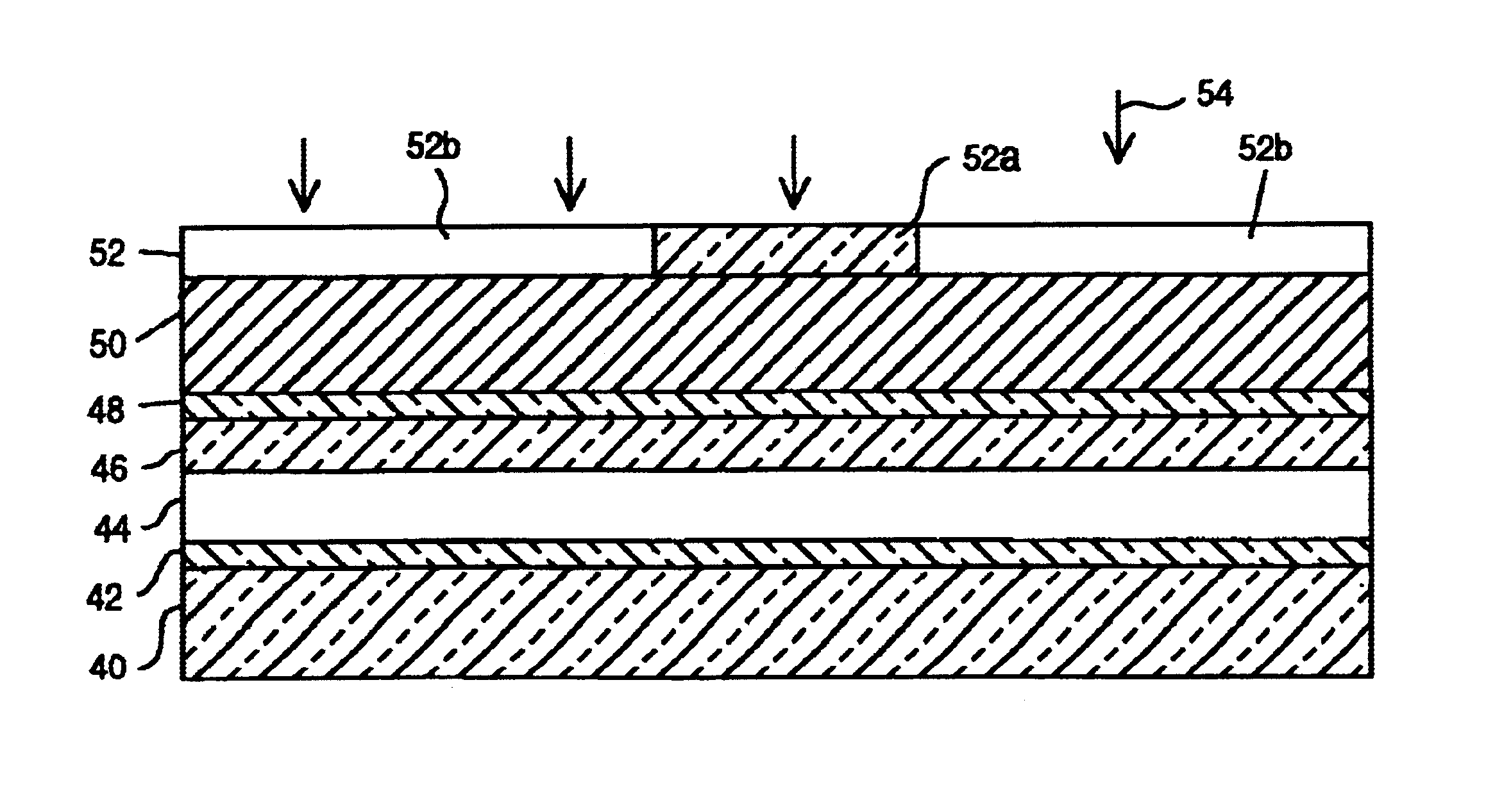
[0073]The silicon oxime layer 46 is formed under the following conditions.[0074]Silane (SiH4) flow rate: 60±10 sccm[0075]Nitrogen flow rate: 400±100 sccm[0076]Nitrous oxide (N2O) flow rate: 40±5 sccm[0077]Pressure: 3.5±0.3 torr[0078]RF power: 150±20 watts[0079]Temperature: 400±10° C.[0080]Processing time: 6±1 seconds (for 300 angstrom thickness)[0081]Spacing (S in FIG. 7) between shower head 72 and surface of wafer 66: 460±20 mils (11.68±0.51 millimeters)[0082]Layer thickness: 200 to 400 angstroms

[0083]After forming the silicon oxime layer 46, the container 62 is pumped down for approximately 10 seconds, and the barrier layer 48 is then grown in-situ on the layer 46. The conditions for growing the barrier layer 48 are as follows.[0084]Nitrous oxide (N2O) flow rate: 190±10 sccm[0085]Pressure: 3.5±0.3 torr[0086]RF power: 150±20 watts[0087]Temperature: 400±10° C.[0088]Processing time: 20±5 seconds

[0089]Spacing (S in FIG. 7) between shower head 72 and surface o...

example ii (

NOVELLUS CONCEPT I System)

[0091]The silicon oxime layer 46 is formed under the following conditions, all of which are variable from the listed values by approximately ±10%.[0092]Silane (SiH4) flow rate: 162 sccm[0093]Nitrogen flow rate: 8,000 sccm[0094]Nitrous oxide (N2O) flow rate: 250 sccm[0095]Pressure: 2.4 torr[0096]RF power: 300 watts[0097]Temperature: 400° C.[0098]Processing time: 2.7 seconds[0099]Soaktime (temperature ramp-up time): 30 seconds

[0100]Spacing (S in FIG. 7) between shower head 72 and surface of wafer 66: 550 mils (13.97 millimeters)[0101]Layer thickness: 300 angstroms

[0102]After forming the silicon oxime layer 46, the container 62 is pumped down for approximately 10 seconds, and the barrier layer 48 is then grown in-situ on the layer 46. The conditions for growing the barrier layer 48 are as follows.[0103]Nitrous oxide (N2O) flow rate: 700 sccm[0104]Pressure: 2.4±0.3 torr[0105]RF power: 750 watts[0106]Temperature: 400° C.[0107]Processing time: 15 seconds

[0108]Spa...

example

[0123]A silicon oxime film was formed by PECVD in a conventional PECVD reactor under the following conditions:

[0124]

temperature400° C.pressure2.5 Torrpower190 wattsGap425 milsSiH450-60 sccmN2O35-45 sccmN2500 sccm

[0125]Under the above conditions, the deposition rate was about 75-85 Å / sec. and the uniformity measured at 1 to 2%, 1σ. Upon analysis, the silicon oxime was found to contain about 15 to about 20 atom percent oxygen, and about 10% to about 20 atom percent hydrogen. A silicon oxime film formed under the above conditions displays absorption characteristics at 365 nm very different from conventional silicon oxynitride films. For example, a silicon oxime film having a thickness of about 350 Å to about 400 Å on polysilicon exhibits a reflectivity of about 1 to 5%; whereas, in order to achieve the same level of reflectivity, i.e., about 1 to about 5%, a conventional silicon oxynitride film requires a thickness of about 700 Å to about 1100 Å.

[0126]It was unexpectedly found that in ...


PUM


Abstract

An anti-reflective coating is formed between a material layer which is to be patterned on a semiconductor structure using photolithography, and an overlying photoresist layer. The anti-reflective coating suppresses reflections from the material layer surface into the photoresist layer that could degrade the patterning. The anti-reflective coating includes an anti-reflective layer of silicon oxime, silicon oxynitride, or silicon nitride, and a barrier layer which is grown on the anti-reflective layer using a nitrous oxide plasma discharge to convert a surface portion of the anti-reflective layer into silicon dioxide. The barrier layer prevents interaction between the anti-reflective layer and the photoresist layer that could create footing. The anti-reflective layer is deposited on the material layer using Plasma Enhanced Chemical Vapor Deposition (PECVD) in a reactor. The barrier layer is grown on the anti-reflective layer in-situ in the same reactor, thereby maximizing throughput.

Description

CROSS-REFERENCE TO RELATED APPLICATION[0001]This application is a continuation-in-part of U.S. patent application Ser. No. 08 / 479,718, filed Jun. 7, 1995, entitled “SILICON OXIME FILM”, by David K. Foote et al, now U.S. Pat. No. 5,710,067, issued Jan. 20, 1998.BACKGROUND OF THE INVENTION[0002]1. Field of the Invention[0003]The present invention generally relates to the art of microelectronic integrated circuits, and more specifically to a process for forming a bottom anti-reflection coating for semiconductor fabrication photolithography which inhibits photoresist footing.[0004]2. Description of the Related Art[0005]Photolithography is a semiconductor fabrication process that is widely used. for patterning material layers on a semiconductor wafer or structure. The material layers can be non-metal (e.g. silicon, polysilicon), metal (e.g. aluminum), etc.[0006]A layer of photoresist is formed over the material layer to be patterned, and exposed to light through a mask which has opaque a...

Claims


Application Information

Patent Timeline
IPC IPC(8): H01L21/02H01L23/52H01L23/522H01L21/027H01L21/70H01L21/314H01L21/768H01L21/312
CPCH01L21/0276H01L21/3121H01L21/3144H01L23/5226H01L21/76802H01L21/76895H01L21/3145H01L2924/0002H01L21/02126H01L21/02274H01L21/0234H01L21/02362H01L21/02164H01L21/0217H01L21/0214H01L2924/00
Inventor FOOTE, DAVID K.NGO, MINH VAN
Owner GLOBALFOUNDRIES INC
Why Eureka
Try Eureka