Photolithographically-patterned variable capacitor structures and method of making

a variable capacitor and photolithographic pattern technology, applied in variable capacitors, feed-through capacitors, fixed capacitors, etc., can solve the problems of high cost, high cost, labor-intensive substrate b>1/b>, etc., and achieve the effect of speed and ease of solder-bump flip-chip bonding

Inactive Publication Date: 2005-07-26
XEROX CORP
View PDF16 Cites 52 Cited by
  • Summary
  • Abstract
  • Description
  • Claims
  • Application Information

AI Technical Summary

Benefits of technology

[0026]Accordingly, this invention provides a spring contact which exhibits the speed and ease of solder-bump flip-chip bonding while eliminating the need to create uniform solder bumps or uniform contacting pressure. This invention further provides a spring contact which has elastic properties enabling the spring contact to maintain physical contact with a contact pad despite variations in contact pad heights...

Problems solved by technology

Since the chip 2 typically has tens or even hundreds of the contact pads 3, wire bonding each contact pad 3 on the chip 2 to the corresponding contact pad 3 on the substrate 1 is labor intensive, expensive and slow.
Like wire bonding, tab bonding suffers from yield loss and high cost.
Irregularities in the heights of the contact pad 3 result in non-uniform contacting force pressing the flexible substrate 5 against the contact pads 3.
The non-uniform contacting force means that some contact pads 3 will not be properly bonded to the flexible substrate 5.
However, flip-chip bonding does suffer from both mechanical and thermal variations in the solder bumps 6.
However, standard techniques for producing the probe card 7 are time consuming and labor-intensive.
Because the probe cards 7 are custom-made and relatively expensive, the probe cards 7 are not typically made to contact all of the contact pads 3 on the device 10 at one time.
These currents cause resistive dissipation that contributes to the coil losses.
The second problem arises when the coil is operated at high frequencies, where skin and proximity effects force the coil current to flow along the outer surfaces of the conductor.
However, this approach is not practical as it sacrifices structural in...

Method used


Image

  • Photolithographically-patterned variable capacitor structures and method of making
  • Photolithographically-patterned variable capacitor structures and method of making
  • Photolithographically-patterned variable capacitor structures and method of making

Examples


Embodiment Construction

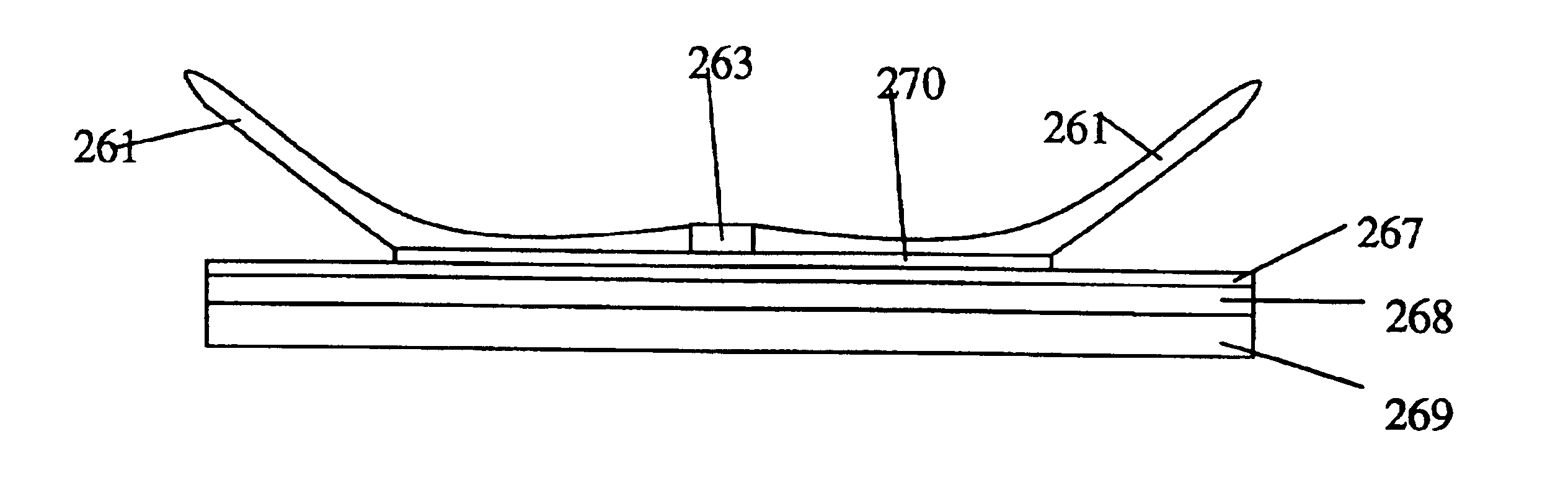
[0097]FIG. 6 shows a side view of a bonding structure 100 having a plurality of spring contacts 15. Each spring contact 15 comprises a free portion 11 and an anchor portion 12 fixed to an underlayer or release layer 13 and electrically connected to a contact pad 3. Each spring contact 15 is made of an extremely elastic material, such as a chrome-molybdenum alloy or a nickel-zirconium alloy. Preferably, the spring contacts 15 are formed of an elastic conductive material, although they can be formed of a non-conductive or semi-conductive material if they are coated or plated with a conductor material. More preferably, the spring contacts 15 are formed of a nickel-zirconium alloy having 1% zirconium. Zirconium is added to the alloy to improve the elastic properties of the alloy while not greatly affecting the conductivity of the alloy. When the elastic material is not conductive, it is coated on at least one side with a conductive material, such as a metal or metal alloy.

[0098]The cont...


PUM


Abstract

A new type of high-Q variable capacitor includes a substrate, a first electrically conductive layer fixed to the substrate, a dielectric layer fixed to a portion of the electrically conductive layer, and a second electrically conductive layer having an anchor portion and a free portion. The anchor portion is fixed to the dielectric layer and the free portion is initially fixed to the dielectric layer, but is released from the dielectric layer to become separated from the dielectric layer, and wherein an inherent stress profile in the second electrically conductive layer biases the free portion away from the dielectric layer. When a bias voltage is applied between the first electrically conductive layer and the second electrically conductive layer, electrostatic forces in the free portion bend the free portion towards the first electrically conductive layer, thereby increasing the capacitance of the capacitor.

Description

[0001]This application is a divisional patent application of U.S. patent application Ser. No. 09 / 573,363, filed on May 17, 2000, now U.S. Pat. No. 6,396,677.BACKGROUND OF THE INVENTION[0002]1. Field of the Invention[0003]This invention generally relates to photolithographically-patterned, out-of-plane coil structures for use in integrated circuits, circuit boards and other devices.[0004]2. Description of Related Art[0005]Standard bonding techniques for electrically connecting integrated circuits, or chips, to a circuit board or other device include wire bonding, tab bonding, and solder-bump flip-chip bonding. FIG. 1 shows a contact pad 3 formed on a chip 2 wire bonded to a corresponding contact pad 3 formed on a substrate 1. The contact pads 3 are electrically connected, or bonded, by a wire 4. Since the chip 2 typically has tens or even hundreds of the contact pads 3, wire bonding each contact pad 3 on the chip 2 to the corresponding contact pad 3 on the substrate 1 is labor intens...

Claims


Application Information

Patent Timeline
IPC IPC(8): H01G5/00H01G5/16H01G17/00H01G7/00
CPCH01G5/16H01G5/18H01F17/0006H01F17/02
Inventor CHUA, CHRISTOPHER L.PEETERS, ERICVAN SCHUYLENBERGH, KOENRAAD F.SMITH, DONALD L.
Owner XEROX CORP
Why Eureka
Try Eureka