
Light emitting apparatus provided with fluorescent substance and semiconductor light emitting device, and method of manufacturing the same

a technology fluorescent substance, which is applied in the direction of discharge tube/lamp details, discharge tube luminescnet screens, natural mineral layered products, etc., can solve the problems of device capable of emitting or receiving light of such a high energy level being particularly prone to uneven color, prone to uneven illumination, etc., to achieve easy manufacturing of light emitting apparatus, easy to grasp the dispersion state, easy to handle resin

Inactive Publication Date: 2005-08-02
NICHIA CORP
View PDF15 Cites 83 Cited by
  • Summary
  • Abstract
  • Description
  • Claims
  • Application Information

AI Technical Summary

Benefits of technology

[0007]With the background described above, an object of the present invention is to provide a light emitting apparatus that is capable of emitting light with uniform and high luminance for a long period of time with less color unevenness, and a method of manufacturing the same.
[0022]The powdered resin is preferably an epoxy resin derived from triazine, and particularly an epoxy resin having an isocyanturate ring. The epoxy resin derived from triazine causes the curing reaction at a very high rate when converted into liquid by heating to a temperature higher than a melting point. Therefore, poor curing of the resin can be prevented even in case the color converting member is applied to form a thin film using a volatile curing agent such as acid anhydride curing agent. Therefore, a light emitting apparatus having high reliability can be manufactured by controlling a mixing ratio of the epoxy resin to the acid anhydride curing agent to a value closer to a stoichiometric number. To supplement volatilization of a small amount of the acid anhydride curing agent, a curing solution may contain an acid anhydride in the amount which is slightly larger than a stoichiometric number of the epoxy compound to be cured.

Problems solved by technology

However, in the light emitting apparatus of the prior art described above, luminance tends to undergo chronological change after an extended period of use, and unevenness in color tends to occur.
A semiconductor device capable of emitting or receiving light of such a high energy level is particularly prone to chronological change in luminance and color unevenness.
However, since the acid anhydride curing agent requires a relatively long curing time, it is prone to absorption of moisture and evaporation during the curing process.
This results in larger area of contact between the resin solution that has been applied and the ambient air, thus making the curing agent more likely to evaporate.
When the color converting member 5 is formed from an epoxy resin solution containing the acid anhydride curing agent, for example, there may occur such a case that the acid anhydride curing agent evaporates and the epoxy resin cannot be normally cured.

Method used


Image

  • Light emitting apparatus provided with fluorescent substance and semiconductor light emitting device, and method of manufacturing the same
  • Light emitting apparatus provided with fluorescent substance and semiconductor light emitting device, and method of manufacturing the same
  • Light emitting apparatus provided with fluorescent substance and semiconductor light emitting device, and method of manufacturing the same

Examples


example 1

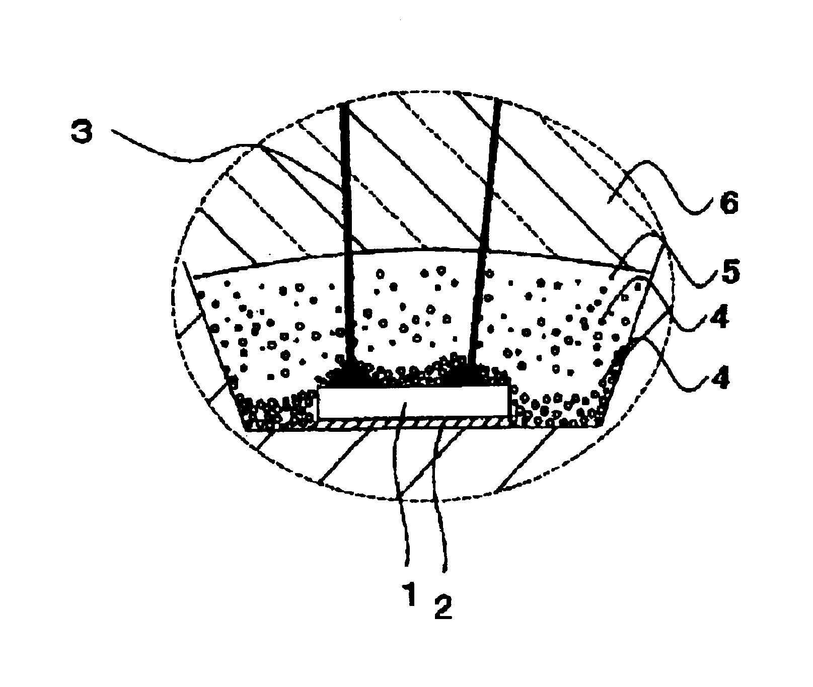
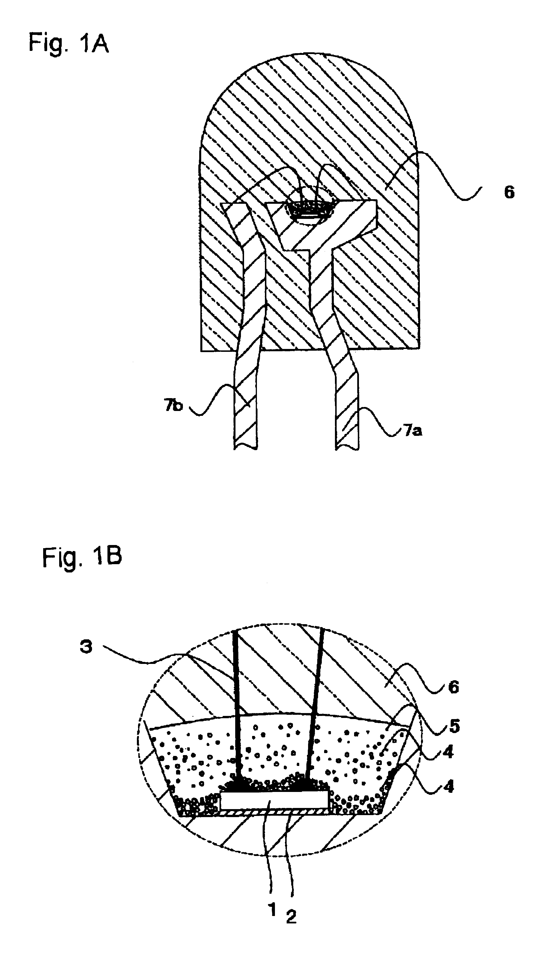
[0069]As the light emitting apparatus of the present invention, a lamp-type light emitting diode of long wavelength converting type is formed as shown in FIGS. 1A and 1B. An LED chip that has a light emitting layer made of InGaN and has main light emission peak at 470 nm is used. The LED chip is formed by the MOCVD process. Specifically, a cleaned sapphire substrate is placed in a reaction chamber. TMG (trimethyl) gas, TMI (trimethyl-indium) gas, TMA (trimethyl-aluminum) gas or ammonia gas is used as the film forming reaction gas, hydrogen gas is used as the carrier gas, and silane gas and cyclopentadiamagnesium is used as the impurity gas.

[0070]The LED chip 1 has such a layer constitution formed on the sapphire substrate, as low-temperature buffer layer of AlGaN, undoped GaN (about 15000 Å thick) for improving crystallinity, Si-doped GaN (about 21650 Å thick) having electrode formed thereon and serves as n-type contact layer, undoped GaN (about 3000 Å thick) for improving crystalli...

example 2

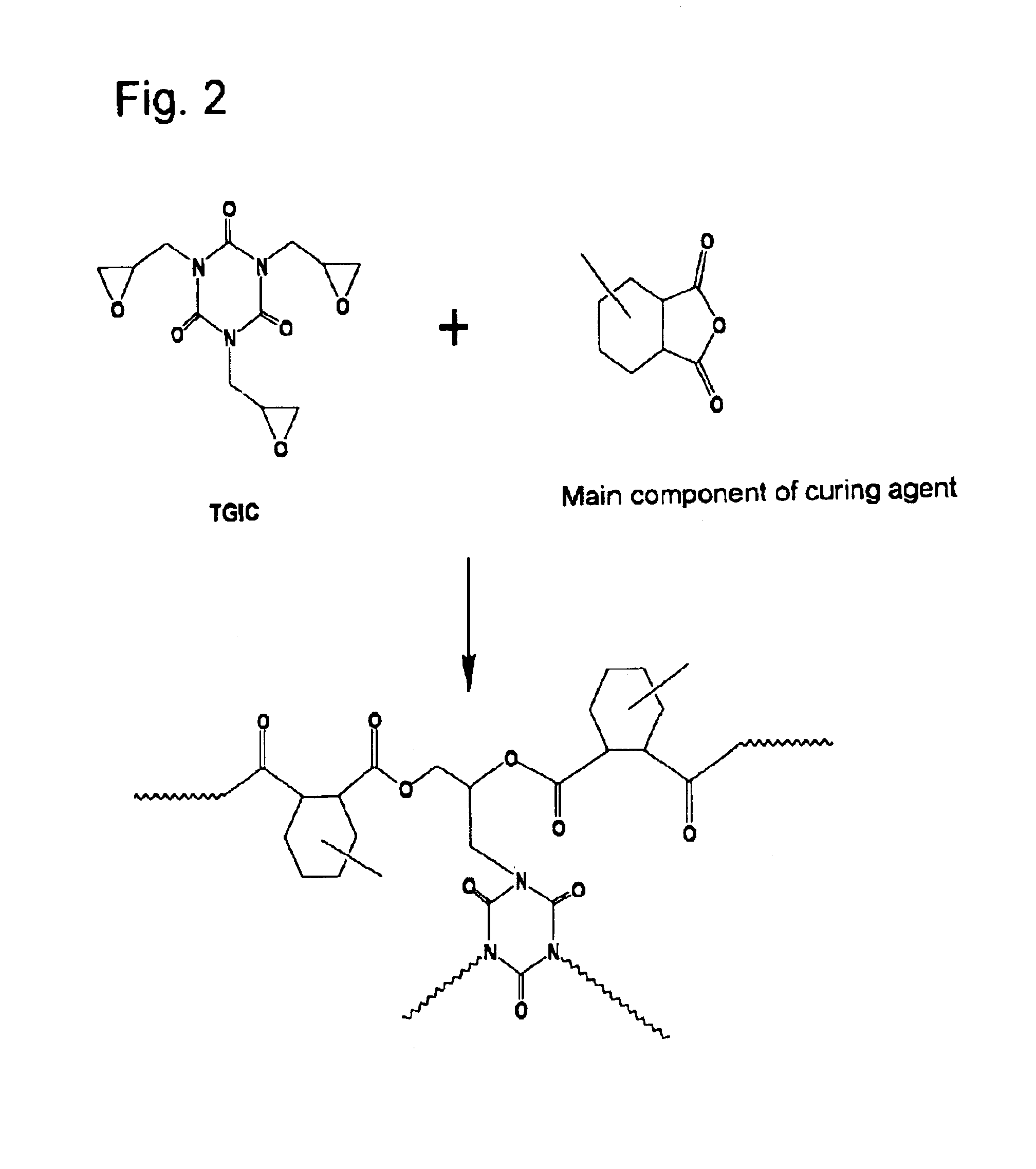
[0082]100 Parts by weight of 1,3,5-triglycidyl isocyanurate, which is an epoxy resin derived from triazine as a base agent, and 328.32 parts by weight of the above curing solution (epoxy equivalent ratio of epoxy resin derived from triazine to the curing agent is 1:2) were mixed to prepare a mixed solution. The resulting mixed solution was mixed with the above fluorescent substance and SiO2 having a center particle diameter of 0.5 μm at a mixing ratio of 100:23:35 and then uniformly dispersed in a ball mill for 24 hours to obtain a dispersion. In the same manner as in Example 1, except that the dispersion was prepared as described above, a light emitting diode was manufactured. As shown in FIG. 5, the same effect as that in Example 1 can be obtained.

example 3

[0083]100 Parts by weight of 1,3,5-triglycidyl isocyanurate, which is an epoxy resin derived from triazine as a base agent, and 328.32 parts by weight of the curing agent were mixed to prepare a mixed solution. The resulting mixed solution was mixed with the fluorescent substance, SiO2 and a diluent at a mixing ratio of 100:23:35:10 and then uniformly dispersed in a ball mill for 24 hours to obtain a dispersion. In the same manner as in Example 1, except that the dispersion was prepared as described above, a light emitting diode was manufactured. As a result, the same effect as that in Example 1 can be obtained.


PUM

PropertyMeasurementUnit
Ratioaaaaaaaaaa
Wavelengthaaaaaaaaaa

Abstract

In a light emitting apparatus comprising a light emitting device, a fluorescent substance capable of absorbing at least a portion of light emitted by the light emitting device and emitting light having a different wavelength, and a color converting member which contains the fluorescent substance and directly coat the light emitting device, the color converting member contains at least an epoxy resin derived from triazine and a mixing ratio of the epoxy resin derived from triazine to the acid anhydride curing agent in the color converting member is from 100:80 to 100:240.

Description

TECHNICAL FIELD[0001]The present invention relates to a light emitting apparatus that can be used as back light, light source for an illuminating switch, display and indicator. Particularly, the present invention relates to a light emitting apparatus capable of emitting light with high luminance over a long period of use.BACKGROUND ART[0002]Semiconductor light emitting device such as LED and LD (laser diode) are small in size and emits light of clear color efficiently. Also as semiconductor devices, they do not burn out, have good drive characteristic and are durable against vibration and repetitive operations of switching ON / OFF. For these reasons, they are used as various indicators and various light sources. However, since such semiconductor light emitting device has monochromatic peak wavelength, it has been necessary to use two or more kinds of semiconductor light emitting device to emit whitish light (white, pink or incandescent-like illumination).[0003]In the meantime, semico...

Claims


Application Information

Patent Timeline
IPC IPC(8): C09K11/06H01L33/00H05B33/14H01L33/50
CPCC09K11/06H01L33/501H05B33/14C09K2211/188H01L2224/32257H01L2224/32245H01L2224/48091H01L2224/48247H01L2224/48465H01L2224/73265H01L2924/00014H01L2924/00H01L2224/8592H01L2224/45144H01L24/45H01L2224/45015H01L2224/45124H01L2224/45147H01L2224/45169H01L2924/20751H01L2924/20752H01L2924/20753H01L2924/20754H01L2924/12042H01L2924/12041H01L2924/181H01L2224/48257H01L2924/00012
Inventor SATO, MASANOBUTSUKIOKA, TOMOYAKURAMOTO, MASAFUMI
Owner NICHIA CORP
Learn More