Low resistivity silicon carbide

a technology of silicon carbide and low resistivity, which is applied in the direction of coating, chemical vapor deposition coating, metallic material coating process, etc., can solve the problems of limited use of high resistivity in other applications, limited use of high resistivity in fabricating components that require a greater degree of electrical conductivity, and restricted use of high resistivity in applications. , to achieve the effect of improving performance, reducing the risk of cracking and low resistivity

Inactive Publication Date: 2005-09-06
TOKAI CARBON CO LTD +1
View PDF9 Cites 6 Cited by
  • Summary
  • Abstract
  • Description
  • Claims
  • Application Information

AI Technical Summary

Benefits of technology

[0018]The present invention is directed to a silicon carbide that has a nitrogen content greater than 3×10¹⁹ atoms / cm3. Advantageously, the silicon carbide of the present invention has a resistivity of less than 0.10 ohm-cm with a variation around an electrical resistivity mean of less than 35%. Such a uniform low resistivity silicon carbide provides for improved performance as furniture in thermal processing methods, and is less susceptible to cracking in extreme environments. Advantageously, the silicon carbide is opaque to light in a wavelength range of from 0.1 μm to 1.0 μm. Silicon carbide of the present invention may be employed as furniture in semi-conductor processing chambers where accurate maintenance of semi-conductor wafer temperatures are desired. Since the low resistivity silicon carbide is opaque at wavelengths of light from 0.1 μm to 1.0 μm, light from heating lamps employed in wafer processing chambers is significantly reduced, thus allowing a more accurate reading of wafer temperatures. Accordingly, defects in wafers caused by improper temperatures are reduced or eliminated.
[0019]Further, because the low resistivity silicon carbide need not be coated with poly-silicon to provide the appropriate opaqueness, such problems as dendritic growth, bread loafing and the high cost of coating are eliminated. Also, the problem of adding thermal mass to silicon carbide articles is eliminated. Thus, faster heating ramp rates for rapid thermal processing are achieved with articles prepared from the low resistivity silicon carbide of the present invention. The faster heating ramp rates in turn provide for reduced total integrated time at high temperatures for wafers and reduced diffusion of dopant during processing.
[0020]The present invention is also directed to a method of making the opaque, low resistivity silicon carbide. The silicon carbide of the present invention is prepared by chemical vapor deposition. Gas phase nitrogen concentrations of at least 56% by volume are employed in the CVD process. Reactants are mixed together with the high concentrations of nitrogen in a CVD chamber, and the silicon carbide product is deposited on a substrate such as a mandrel. Total furnace pressure during the CVD process is at least 300 torr. Surprisingly, by increasing total furnace pressure to at least 300 torr to increase nitrogen concentration, desirable properties such as thermal conductivity, thermal stability and the like are not compromised. Accordingly, the silicon carbide articles may readily be employed CVD and RTP processes.

Problems solved by technology

While this is a desirable characteristic for certain applications, such a characteristic is a limitation restricting its use in other applications.
While high temperature properties of CVD-SiC have made it a material of choice for use in such chambers, its high resistivity has limited its use in fabricating components that require a greater degree of electrical conductivity.
High electrical resistivity of CVD-SiC has further restricted its use in applications that are subject to the buildup of static electricity.
If the plasma is permitted to spread beyond the low resistivity components, it will generate heat in the system which will degrade the equipment.
However, the electrical resistivity of the SiC was not as uniform as the industry preferably desires.
Altering reaction components and chamber conditions may affect the stoichiometry of SiC reactants such that the resulting SiC may have reduced properties, such as thermal conductivity, and may be prone to cracking.
Thus, a worker may not readily predict the quality of SiC that he may obtain by altering reaction parameters based on previous SiC synthesis processes.
While the resistivity of CVD-SiC can theoretically be lowered to a desired level by the introduction of a sufficient amount of impurities, such as boron, the resulting elevated levels of impurities adversely affect other properties of the SiC such as thermal conductivity and / or high temperature stability.
Temperatures in an RTP chamber may exceed 1100° C. and are subject to rapid change, thereby making precise control of the substrate temperature complicated and difficult.
Also, any light from the W-halogen lamps that passes through (transmits) a susceptor or edge ring can cause an incorrect temperature reading by the pyrometer.
However, although opaqueness may be increased, coating edge rings with poly-silicon adds substantial cost to the edge rings.
Further, the coating process (epitaxial silicon growth) has many technical problems associated with it such as dendritic growth, bread loafing around edges and purity problems that reduce yields.
The increased thermal mass limits heating ramp rates during RTP processing cycles.

Method used


Image

  • Low resistivity silicon carbide
  • Low resistivity silicon carbide

Examples


example 1

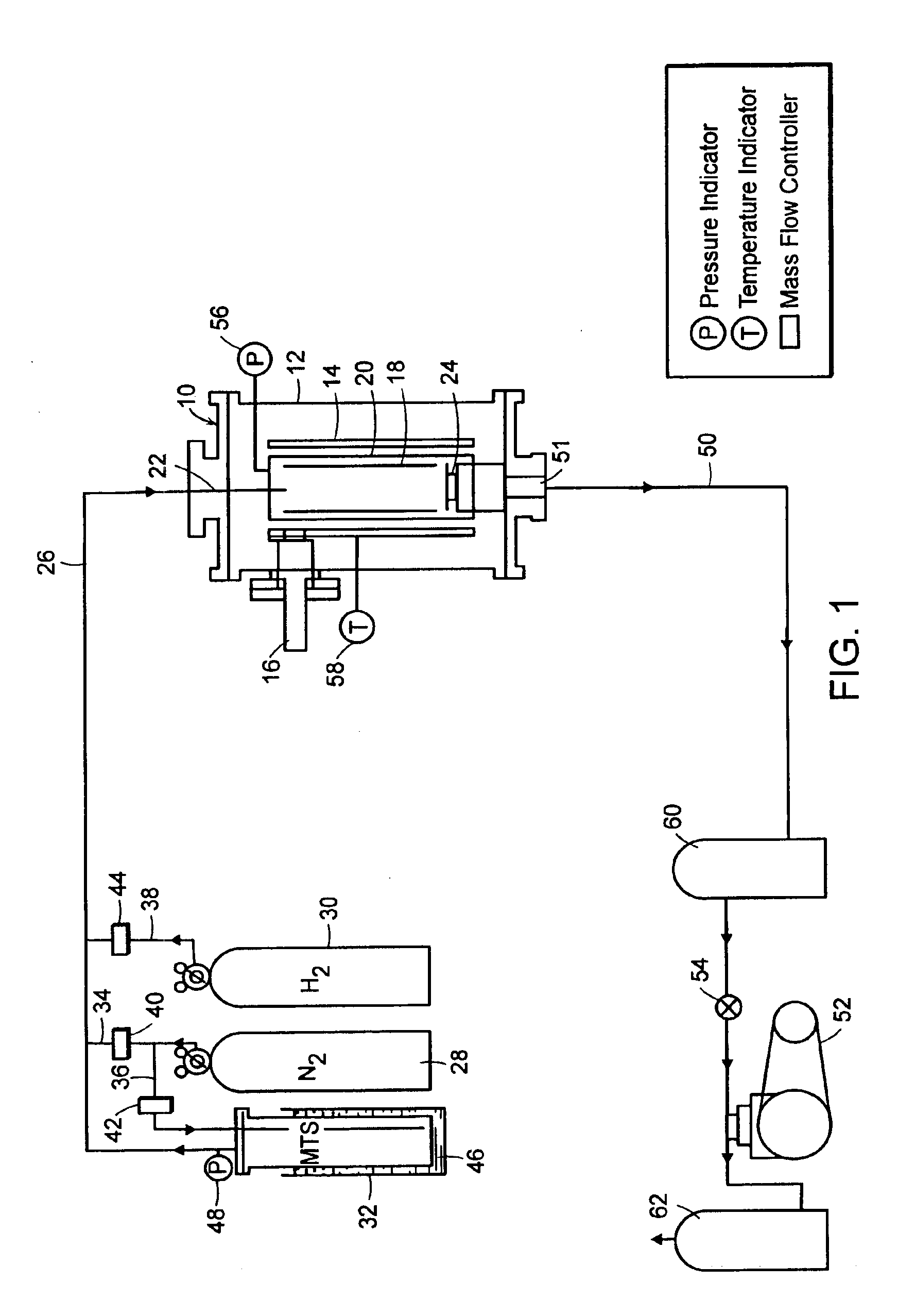
[0049]An opaque, low resistivity silicon carbide was produced according to a method of the present invention in an apparatus similar to that illustrated in FIG. 1 with the following process conditions: deposition temperature=1350° C., total furnace pressure=300 torr, hydrogen partial pressure=92 torr, MTS partial pressure=17 torr, and nitrogen partial pressure=191 torr. The nitrogen partial pressure corresponded to 63.6% of nitrogen in the process. One inch equals 2.54 centimeters. Six resistivity samples were fabricated from different locations in one plate (24×29-inches). The resistivity values fell in the range of 0.057-0.071 ohm-cm. The average electrical resistivity of the six samples was 0.064 ohm-cm. The deposition thickness range was 0.24-0.564-inches yielding a deposition rate of 2.7-6.3 mil / hour. The silicon carbide was characterized for thermal conductivity by laser flash technique, solid phase N2 concentration by secondary ion mass spectroscopy, and purity by gas dischar...

example 2

[0051]An opaque, low resistivity silicon carbide was produced according to a method of the present invention in an apparatus similar to that illustrated in FIG. 1 with the following process conditions: deposition temperature=1350° C., total furnace pressure=400 torr, hydrogen partial pressure=100 torr, MTS partial pressure=16 torr, and nitrogen partial pressure=284 torr. The nitrogen partial pressure corresponded to 72% of nitrogen in the process. Six resistivity samples were fabricated from different locations in one plate (24×29-inches). The resistivity values fell in the range of 0.04-0.043 ohm-cm. The average resistivity of the six samples was 0.041 ohm-cm. The deposition thickness range for 78 hour deposition was 0.172-0.355-inches yielding a deposition rate of 2.2-4.5 mil / hour. The material was characterized as in Example 1 and the results are given below:

[0052]

PropertyValueThermal conductivity227-283 W / mKSolid phase N2 conc.4.2 × 1019 atoms / ccChemical impurity1.85 (ppmw)

The a...

example 3

[0053]An opaque, low resistivity silicon carbide was produced according to a method of the present invention in an apparatus similar to that illustrated in FIG. 1 with the following process conditions: deposition temperature=1350° C., total furnace pressure=650 torr, hydrogen partial pressure=110 torr, MTS partial pressure=17 torr, and nitrogen partial pressure=523 torr. The nitrogen partial pressure corresponds to 80% of nitrogen in the process. Six resistivity samples were fabricated from different locations in one plate (24×29-inches). The resistivity values fell in the range of 0.015-0.028 ohm-cm. The average resistivity was 0.021 ohm-cm. The deposition thickness range for 84 hours of deposition was 0.134-0.302-inches yielding a deposition rate of 1.6-3.6 mil / hour. The material was characterized as in Example 1 and the results are given below:

[0054]

PropertyValueThermal conductivity220-257 W / mKSolid phase N2 conc.7.6 × 1019 atoms / ccChemical impurity2.07 (ppmw)

The above property v...


PUM

PropertyMeasurementUnit
temperaturesaaaaaaaaaa
wavelengthaaaaaaaaaa
absorption coefficientaaaaaaaaaa

Abstract

An opaque, low resistivity silicon carbide and a method of making the opaque, low resistivity silicon carbide. The opaque, low resistivity silicon carbide is doped with a sufficient amount of nitrogen to provide the desired properties of the silicon carbide. The opaque, low resistivity silicon carbide is a free-standing bulk material that may be machined to form furniture used for holding semi-conductor wafers during processing of the wafers. The opaque, low resistivity silicon carbide is opaque at wavelengths of light where semi-conductor wafers are processed. Such opaqueness provides for improved semi-conductor wafer manufacturing. Edge rings fashioned from the opaque, low resistivity silicon carbide can be employed in RTP chambers.

Description

[0001]The present application is a continuation-in-part application of U.S. patent application Ser. No. 09 / 790,442 filed Feb. 21, 2001 which is a non-provisional application of Provisional Application Ser. No. 60 / 184,766 filed Feb. 24, 2000.BACKGROUND OF THE INVENTION[0002]The present invention is directed to an improved low resistivity silicon carbide. More specifically, the present invention is directed to an improved low resistivity silicon carbide that has a high nitrogen concentration.[0003]Silicon carbide (SiC), especially silicon carbide produced by chemical vapor deposition (CVD), has unique properties that make it a material of choice in many high temperature applications. Chemical vapor deposition processes for producing free-standing silicon carbide articles involve a reaction of vaporized or gaseous chemical precursors in the vicinity of a substrate to result in silicon carbide depositing on the substrate. The deposition reaction is continued until the deposit reaches th...

Claims


Application Information

Patent Timeline
Patent Type & Authority Patents(United States)
IPC IPC(8): C23C16/00C23C16/01C23C16/32
CPCC23C16/01C23C16/325
Inventor GOELA, JITENDRA S.PICKERING, MICHAEL A.
Owner TOKAI CARBON CO LTD
Why Eureka
Try Eureka