Manufacturing system and apparatus for balanced product flow with application to low-stress underfilling of flip-chip electronic devices

a flip-chip electronic device and product flow technology, applied in the field of electronic systems and semiconductor devices, can solve the problems of delaminate the solder joint, create thermomechanical stress on its own, and event-driven assembly failure, and achieve low-stress, reliable products, and reduce manufacturing costs

Active Publication Date: 2005-12-20
TEXAS INSTR INC
View PDF4 Cites 9 Cited by
  • Summary
  • Abstract
  • Description
  • Claims
  • Application Information

AI Technical Summary

Benefits of technology

[0012]On command, the pallet is withdrawn from the waiting line and moved into a third workstation suitable to complete the polymerization of the precursor, where the precursor is completely polymerized. Finally, the completed assembly is cooled to ambient temperature. All heating and cooling steps are performed at computer-controlled ramp rates. The temperature ramps, together with the constant temperature waiting periods, are designed to relieve thermomechanical stress.
[0013]Embodiments of the present invention are related to solder-ball and bump-bonded IC assemblies, semiconductor device packages, surface mount and chip-scale packages. It is a technical advantage that the invention offers a flexible and high-throughput assembly methodology resulting in very low-stress, reliable products. It is an additional technical advantage that the invention uses a chamber for balancing the production line flow, which is general enough in its concept and features that it permits insertion into the production flow at various stages of the flow. Further technical advantages include the opportunity to scale the assembly to smaller dimensions and mechanically weaker materials, supporting the ongoing trend of IC miniaturization, and to distribute the chip contacts more evenly over the chip area rather than restricting the contacts to a linear arrangement along the chip perimeters, supporting the ongoing trend towards higher input / output count.

Problems solved by technology

These stresses tend to fatigue the joints and the bumps, resulting in cracks and eventual failure of the assembly.
It is well known in the industry that the temperature cycling needed for this curing process can create thermomechanical stress on its own, which may be detrimental to the chip and / or the solder interconnections.
For example, the stress created by a cooling step after reflow just prior to the underfill process, and by cooling after the underfill curing step may delaminate the solder joint, crack the passivation of the chip, or propagate fractures into the circuit structures.
In general, the sensitivity to cracking of the layered structures of integrated circuits increases strongly with decreasing thickness of the various layers and increasing mechanical weakness of low dielectric constant insulators.

Method used


Image

  • Manufacturing system and apparatus for balanced product flow with application to low-stress underfilling of flip-chip electronic devices
  • Manufacturing system and apparatus for balanced product flow with application to low-stress underfilling of flip-chip electronic devices
  • Manufacturing system and apparatus for balanced product flow with application to low-stress underfilling of flip-chip electronic devices

Examples


Embodiment Construction

[0027]The present invention is related to U.S. Pat. No. 6,213,347, issued Apr. 10, 2001, and U.S. Pat. No. 6,228,680, issued May 8, 2001 (Thomas, “Low Stress Method and Apparatus for Underfilling Flip-Chip Electronic Devices”); and U.S. Pat. No. 6,245,583, issued Jun. 12, 2001 (Amador et al., “Low Stress Method and Apparatus of Underfilling Flip-Chip Electronic Devices”).

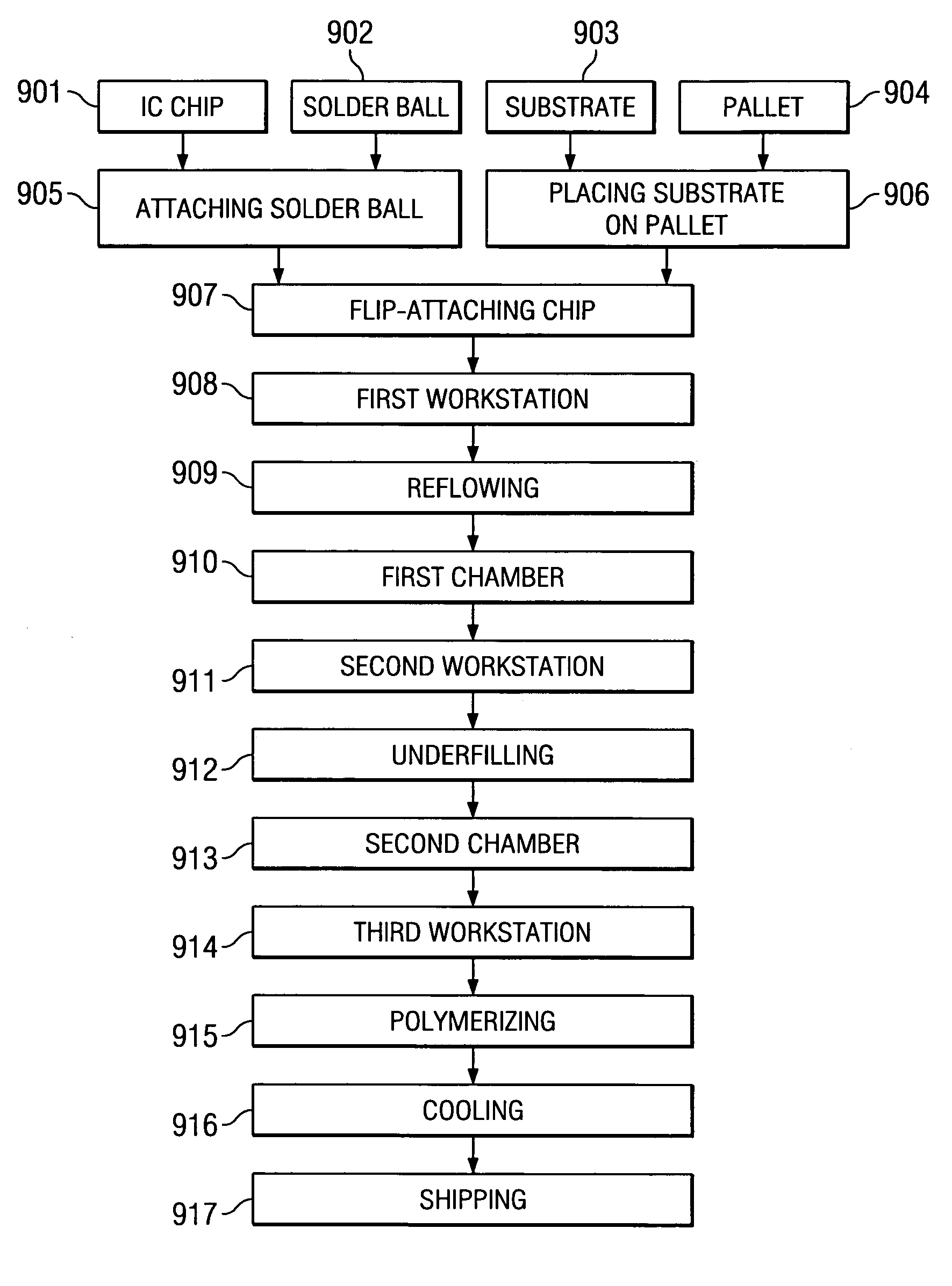
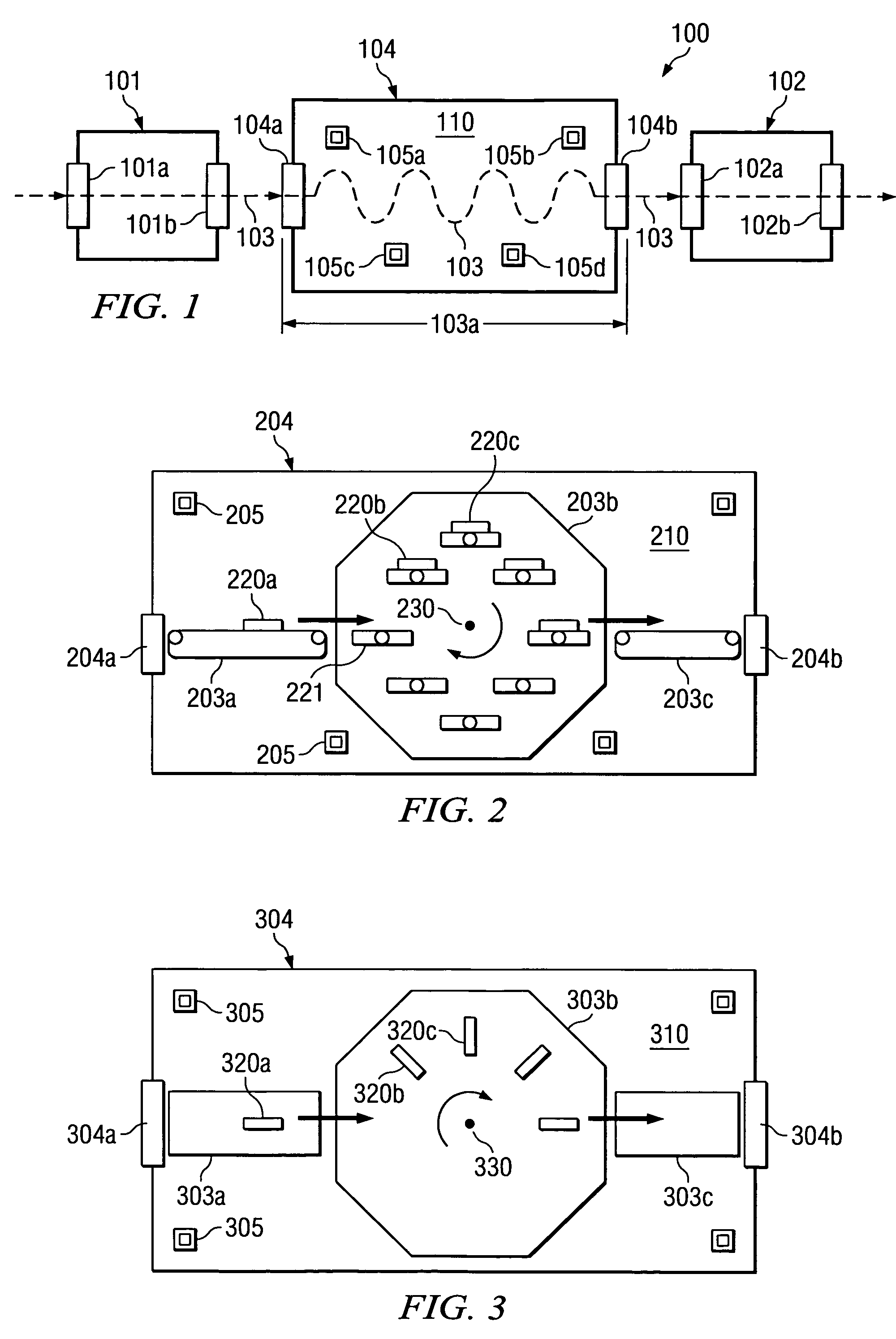
[0028]To illustrate an embodiment of the invention, FIG. 1 depicts schematically a group 100 of workstations and other systems as they are arranged consecutively to form a portion of the fabrication process flow for certain products. The direction of the manufacturing flow is indicated in FIG. 1 by the dashed arrows 103. An example of such product and fabrication flow in semiconductor technology is the assembly of integrated circuit chips onto substrates using the flip-chip process.

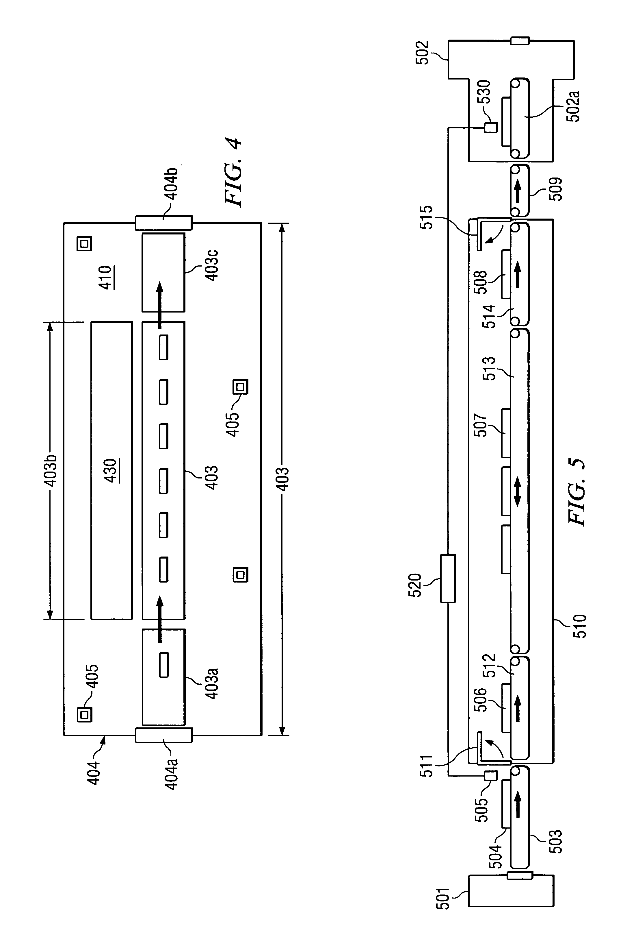
[0029]In FIG. 1, a first workstation 101 has a first entry 101a and a first exit 101b. Workstation 101 serves to perform a specific manu...


PUM


Abstract

A system (100) for manufacturing product, in which a first work station (101) is operable to perform a first manufacturing action on the product parts; this first station has a first entrance (101a) and a first exit 101b). A second work station (102) is operable to perform a second manufacturing action on the product parts; this second station has a second entrance (102a) and a second exit (102b). A transport line (103) between the first exit and the second entrance is operable to move the product parts under computer control. A chamber (104) encloses a portion of the line and is constructed so that the transport achieves a balanced throughput from the first station to the second station, while the product parts are exposed to computer-controlled environmental conditions (110) during transport through the chamber. The balanced throughput in the chamber is achieved by waiting lines for the product with computer-controlled monitors (105a) for product parts' positions and times in the chamber.

Description

FIELD OF THE INVENTION[0001]The present invention is related in general to the field of electronic systems and semiconductor devices and more specifically to an apparatus for enhancing process control and reducing thermomechanical stress in the assembly of semiconductor devices.DESCRIPTION OF THE RELATED ART[0002]When an integrated circuit (IC) chip is assembled on an insulating substrate with conducting lines, such as a printed circuit board, by solder bump connections, the chip is spaced apart from the substrate by the bumps, thereby forming a gap between the chip and substrate. The IC chip is typically a semiconductor such as silicon, silicon germanium, or gallium arsenide, the substrate is usually made of ceramic or polymer-based materials such as FR-4. Consequently, there is a significant difference between the coefficients of thermal expansion (CTE) of the chip and the substrate; for instance, with silicon (about 2.5 ppm / ° C.) as the semiconductor material and plastic FR-4 (ab...

Claims


Application Information

Patent Timeline
Patent Type & Authority Patents(United States)
IPC IPC(8): B65G49/07G06F7/00H01LH01L21/00H01L21/44H01L21/56H01L21/60H01L23/02
CPCH01L21/563H01L21/67236H01L24/75H01L24/81H01L2224/13111H01L2224/73203H01L2224/75H01L2224/81801H01L2924/01013H01L2924/01029H01L2924/01032H01L2924/01033H01L2924/01046H01L2924/01047H01L2924/01079H01L2924/01082H01L2924/10329H01L2924/14H01L2924/01005H01L2924/01006H01L2924/01019H01L2924/0105H01L2924/01087H01L2924/014H01L2924/10253H01L2924/00H01L2224/05573H01L2224/05655H01L2224/05664H01L2924/15787H01L2924/00014H01L21/56H01L23/28
Inventor ODEGARD, CHARLES A.YAMUNAN, VINUCHIU, TZ-CHENG
Owner TEXAS INSTR INC
Why Eureka
Try Eureka