

Laser diode and semiconductor light-emitting device producing visible-wavelength radiation
- Summary
- Abstract
- Description
- Claims
- Application Information
AI Technical Summary
Benefits of technology
Problems solved by technology
Method used
Image

Examples
tenth embodiment
[Tenth Embodiment]
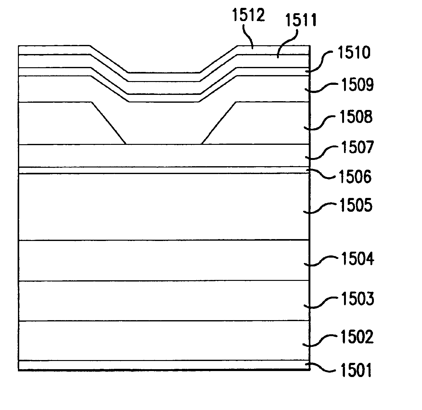
[0386]FIG. 19 shows the construction of a laser diode according to a tenth embodiment of the present invention.
[0387]Referring to FIG. 19, the laser diode is constructed on a substrate 1702 of n-type GaAs carrying thereon a composition-graded layer. 1703 of n-type GaAsP having a composition represented as GaAsyP1−y, wherein the composition-graded layer 1703 is formed by an MOCVD process while changing the composition y continuously and gradually from 1 to 0.4. The growth process of the composition-graded layer 1703 is well established a smooth surface is realized by optimizing the composition gradient.
[0388]Next, a buffer layer 1704 of n-type GaAsP having a composition of GaAs0.6P0.4 is grown on the composition-graded layer 1703, and a cladding layer 1705 of n-type AlGaInAsP, an active layer 1706 of undoped GaInAsP, a first cladding layer 1707 of p-type AlGaInAsP, an etching stopper layer 1708 of p-type GaInAsP, and a current confinement layer 1709 of n-type AlInAs...
eleventh embodiment
[Eleventh Embodiment]
[0398]FIG. 20 shows the construction of a laser diode according to an eleventh embodiment of the present invention.
[0399]Referring to FIG. 20, the laser diode is constructed on a substrate 1802 of n-type GaAs carrying thereon a composition-graded layer 1803 of n-type GaAsP having a composition represented as GaAsyP1−y, wherein the composition-graded layer 1803 is formed by an MOCVD process while changing the composition y continuously and gradually from 1 to 0.4. The growth process of the composition-graded layer 1803 is well established a smooth surface is realized by optimizing the composition gradient.
[0400]Next, a buffer layer 1804 of n-type GaAsP having a composition of GaAs0.6P0.4 is grown on the composition-graded layer 1803, and a cladding layer 1805 of n-type AlGaInAsP, an active layer 1806 of undoped GaInAsP, a first cladding layer 1807 of p-type AlGaInAsP, an etching stopper layer 1808 of p-type GaInAsP, a current confinement layer 1809 of n-type AlIn...
twelfth embodiment
[Twelfth Embodiment]
[0409]FIG. 21 shows the construction of a laser diode according to a twelfth embodiment of the present invention.
[0410]Referring to FIG. 21, the laser diode is constructed on a substrate 1902 of n-type GaAs carrying thereon a composition-graded layer 1903 of n-type GaAsP having a composition represented as GaAsyP1−y, wherein the composition-graded layer 1903 is formed by an MOCVD process while changing the composition y continuously and gradually from 1 to 0.4. The growth process of the composition-graded layer 1903 is well established a smooth surface is realized by optimizing the composition gradient.
[0411]Next, a buffer layer 1904 of n-type GaAsP having a composition of GaAs0.6P0.4 is grown on the composition-graded layer 1903, and a cladding layer 1905 of n-type AlGaInAsP, an optical waveguide layer 1906 of undoped GaInP, an active layer 1907 of undoped GaInAsP, an optical waveguide layer 1908 of undoped GaInP, a first current-blocking layer 1909 of p-type Al...
PUM
 Abstract
Description
Claims
Application Information